

Lattice Semiconductor
ICE65L01F-TQN84I
FPGAs

Not available to buy online? Want the lower wholesale price? Please Send RFQ to get best price, we will respond immediately


.png?x-oss-process=image/format,webp/resize,p_30)


ICE65L01F-TQN84I Description
Lattice Semiconductor's ICE65L01F-TQN84I is a high-performance programmable logic device designed to meet the demands of various applications. This device is part of Lattice's iCE65 family of FPGAs, which are known for their low power consumption, small form factor, and high integration.
Description:
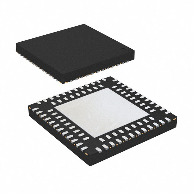
The ICE65L01F-TQN84I is a Field Programmable Gate Array (FPGA) that comes in a compact 8.4mm x 8.4mm TQFP package with 84 pins. It is based on Lattice's low-power 65nm technology and provides a combination of general-purpose and dedicated logic resources to enable flexible and efficient design implementation.
Features:
- Low power consumption: The ICE65L01F-TQN84I is designed to operate with low power consumption, making it suitable for battery-powered and energy-sensitive applications.
- Small form factor: The compact 8.4mm x 8.4mm TQFP package allows for easy integration into space-constrained systems.
- High integration: The device offers a high level of integration, combining general-purpose and dedicated logic resources to provide a versatile solution for various applications.
- Versatile I/O options: The ICE65L01F-TQN84I provides a wide range of I/O options, including LVCMOS, LVDS, and serdes, to support various interface requirements.
- Configurable logic blocks: The device features configurable logic blocks that can be programmed to implement a wide range of functions, providing flexibility in design implementation.
- On-chip memory: The ICE65L01F-TQN84I includes on-chip memory resources, such as block RAM and register files, to support data storage and processing requirements.
- Security features: The device offers security features, such as encryption and authentication, to protect intellectual property and ensure data integrity.
Applications:
The ICE65L01F-TQN84I is suitable for a wide range of applications due to its low power consumption, small form factor, and high integration. Some potential applications include:
- Industrial control systems: The device can be used in industrial control systems for tasks such as motor control, sensor interfacing, and data acquisition.
- Consumer electronics: The ICE65L01F-TQN84I can be used in consumer electronics, such as smartphones, tablets, and wearable devices, for functions like image processing, audio processing, and user interface control.
- Automotive systems: The device can be used in automotive systems for applications like infotainment, driver assistance, and safety systems.
- Communications infrastructure: The ICE65L01F-TQN84I can be used in communication systems for functions like signal processing, data conversion, and network management.
- Medical devices: The device can be used in medical devices for applications like imaging, patient monitoring, and diagnostics.
- Security systems: The ICE65L01F-TQN84I can be used in security systems for functions like encryption, authentication, and access control.
In summary, Lattice Semiconductor's ICE65L01F-TQN84I is a versatile and high-performance FPGA that offers low power consumption, a small form factor, and a wide range of features suitable for various applications across different industries.
Tech Specifications
ICE65L01F-TQN84I Documents
Download datasheets and manufacturer documentation for ICE65L01F-TQN84I
ICE65 Ultra Low-Pwr FPGA Package Diagrams Leaded Pkg PCB Layout Guide All Dev Pkg Mark Chg 12/Nov/2018 iCE65 Family 11/Apr/2012 Top Mark Format Change 20/Dec/2023 Related Parts


Relevant Search
Shopping Guide


.png?x-oss-process=image/format,webp/resize,h_32)


©2025 ERSA Electronics Corporation.