
 German
 Japanese
 Portuguese
 Korea
Korea
 Mexico
 Dutch
Dutch


Lattice Semiconductor
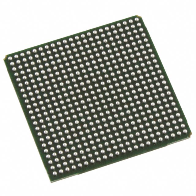
LFXP2-40E-5FN484C

Why Choose Us?
Professional Platform
B2B & B2C purchasingDelivery at full speed
1-2 days deliveryWide variety
Original manufacturers365 days guarantee
Responsible quality
.png)


Tech Specifications
LFXP2-40E-5FN484C Description
Lattice Semiconductor's LFXP2-40E-5FN484C is a high-performance programmable logic device that offers a range of features and applications for various industries.
Description:
The LFXP2-40E-5FN484C is a field programmable gate array (FPGA) that is designed to provide high-density integration and low power consumption. It is based on Lattice's advanced low power FPGA technology and is available in a 5x5mm fine pitch ball grid array (FBGA) package.
Features:
- High-density integration: The LFXP2-40E-5FN484C offers a high-density integration of logic elements, memory, and I/O, making it suitable for a wide range of applications.
- Low power consumption: The device is designed to operate at low power, making it ideal for battery-powered and energy-sensitive applications.
- Versatile I/O options: The LFXP2-40E-5FN484C provides a wide range of I/O options, including LVDS, DDR, and SerDes, making it suitable for various interface requirements.
- Security features: The device includes advanced security features, such as encryption and authentication, to protect sensitive data and intellectual property.
- Configuration flexibility: The LFXP2-40E-5FN484C can be configured and reconfigured in the field, providing flexibility and adaptability for changing requirements.
Applications:
The LFXP2-40E-5FN484C is suitable for a wide range of applications, including:
- Industrial control and automation: The device can be used in industrial control systems, such as motor control, sensor interfacing, and data acquisition.
- Communications infrastructure: The LFXP2-40E-5FN484C can be used in communication systems, such as base stations, routers, and switches, to provide high-speed data processing and interface flexibility.
- Consumer electronics: The device can be used in consumer electronics, such as set-top boxes, gaming consoles, and smart home devices, to provide advanced processing capabilities and low power consumption.
- Automotive: The LFXP2-40E-5FN484C can be used in automotive applications, such as infotainment systems, advanced driver assistance systems (ADAS), and body control modules, to provide high-performance processing and robust security features.
- Aerospace and defense: The device can be used in aerospace and defense applications, such as radar systems, satellite communications, and secure communication systems, to provide high reliability and advanced processing capabilities.
In summary, Lattice Semiconductor's LFXP2-40E-5FN484C is a versatile and high-performance FPGA that offers a range of features and applications for various industries. Its high-density integration, low power consumption, and flexible configuration make it an ideal choice for a wide range of applications, from industrial control to aerospace and defense.
FAQ
Not available to buy online? Want the lower wholesale price? Please Send RFQ to get best price, we will respond immediately


.png?x-oss-process=image/format,webp/resize,h_32)


