
 German
 Japanese
 Portuguese
 Korea
Korea
 Mexico
 Dutch
Dutch


Lattice Semiconductor
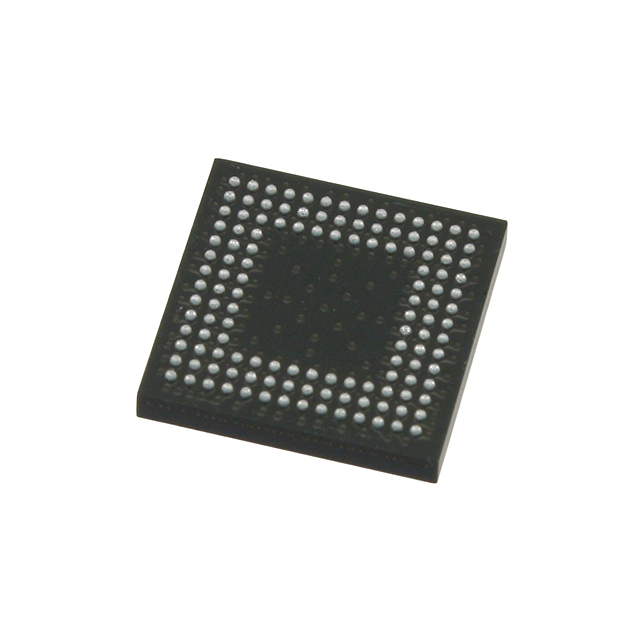
LFXP2-5E-6MN132I

Why Choose Us?
Professional Platform
B2B & B2C purchasingDelivery at full speed
1-2 days deliveryWide variety
Original manufacturers365 days guarantee
Responsible quality
.png)


Tech Specifications
LFXP2-5E-6MN132I Description
Lattice Semiconductor's LFXP2-5E-6MN132I is a powerful programmable logic device that offers a range of features and applications for various industries.
Description:
The LFXP2-5E-6MN132I is a low-cost, high-performance FPGA (Field-Programmable Gate Array) that is designed to meet the needs of a wide range of applications. This device is based on Lattice's advanced 5G technology and is manufactured using a 65nm low-power process. It features a compact 132-ball FBGA package, making it ideal for use in space-constrained applications.
Features:
- Advanced 5G Technology: The LFXP2-5E-6MN132I is based on Lattice's cutting-edge 5G technology, providing high-speed connectivity and low latency for demanding applications.
- 65nm Low-Power Process: Manufactured using a 65nm low-power process, this device offers excellent power efficiency and performance.
- Compact 132-Ball FBGA Package: The compact form factor of the LFXP2-5E-6MN132I makes it suitable for use in space-constrained applications.
- High-Speed Connectivity: With support for high-speed transceivers, this FPGA can handle data rates up to 12.5 Gbps, making it ideal for use in communication and networking applications.
- Versatile I/O Options: The LFXP2-5E-6MN132I offers a wide range of I/O options, including LVDS, DDR, and SerDes, allowing for flexible system design.
- Powerful DSP Blocks: Equipped with powerful DSP blocks, this device can perform complex signal processing tasks with ease.
- Security Features: The LFXP2-5E-6MN132I includes advanced security features, such as encryption and authentication, to protect sensitive data.
Applications:
- Communication and Networking: The LFXP2-5E-6MN132I is well-suited for communication and networking applications, such as 5G base stations, routers, and switches.
- Industrial Automation: This FPGA can be used in industrial automation systems for motor control, sensor interfacing, and data acquisition.
- Automotive: The LFXP2-5E-6MN132I can be used in various automotive applications, such as infotainment systems, advanced driver assistance systems (ADAS), and body control modules.
- Consumer Electronics: This device can be used in consumer electronics, such as set-top boxes, gaming consoles, and smart home devices.
- Aerospace and Defense: The LFXP2-5E-6MN132I is suitable for aerospace and defense applications, such as radar systems, satellite communications, and secure communication systems.
In summary, Lattice Semiconductor's LFXP2-5E-6MN132I is a versatile and powerful FPGA that offers a range of features and applications for various industries. Its advanced 5G technology, compact form factor, and powerful DSP blocks make it an ideal choice for high-speed connectivity and complex signal processing tasks.
FAQ
Not available to buy online? Want the lower wholesale price? Please Send RFQ to get best price, we will respond immediately


.png?x-oss-process=image/format,webp/resize,h_32)


