

Lattice Semiconductor
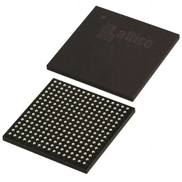
LCMXO2-7000HC-6FTG256I
FPGAs

Not available to buy online? Want the lower wholesale price? Please Send RFQ to get best price, we will respond immediately


.png?x-oss-process=image/format,webp/resize,p_30)


LCMXO2-7000HC-6FTG256I Description
The Lattice Semiconductor's LCMXO2-7000HC-6FTG256I is a high-performance field programmable gate array (FPGA) device that is designed to meet the demanding requirements of various applications.
Description:
The LCMXO2-7000HC-6FTG256I is a member of Lattice Semiconductor's low-cost, low-power, and small form factor FPGA family. It is based on the company's advanced 28 nm process technology and features a high-speed transceiver, which makes it suitable for a wide range of applications.
Features:
The LCMXO2-7000HC-6FTG256I offers several features that make it an attractive choice for various applications. Some of these features include:
- Low power consumption: The device is designed to operate at low power, making it ideal for battery-powered and energy-sensitive applications.
- High-speed transceiver: The device features a high-speed transceiver that supports data rates up to 12.5 Gbps, making it suitable for high-speed communication and data transfer applications.
- Small form factor: The device is available in a compact 256-ball fine pitch ball grid array (FBGA) package, making it suitable for space-constrained applications.
- Versatile I/O options: The device offers a wide range of I/O options, including LVCMOS, LVDS, and serdes, making it suitable for a wide range of applications.
- Security features: The device includes security features such as AES encryption and secure boot, making it suitable for applications that require high levels of security.
Applications:
The LCMXO2-7000HC-6FTG256I is suitable for a wide range of applications, including:
- Communication systems: The high-speed transceiver and versatile I/O options make the device suitable for communication systems such as base stations, routers, and switches.
- Industrial control systems: The low power consumption and small form factor make the device suitable for industrial control systems such as motor control and sensor interfacing.
- Consumer electronics: The device's small form factor and low power consumption make it suitable for consumer electronics such as set-top boxes, gaming consoles, and smart home devices.
- Automotive systems: The device's security features and high-speed transceiver make it suitable for automotive systems such as infotainment systems and advanced driver assistance systems (ADAS).
- Aerospace and defense: The device's high-speed transceiver and security features make it suitable for aerospace and defense applications such as satellite communication systems and secure communication systems.
Overall, the LCMXO2-7000HC-6FTG256I is a versatile FPGA device that offers a range of features that make it suitable for a wide range of applications. Its low power consumption, small form factor, and high-speed transceiver make it an attractive choice for designers looking for a cost-effective and high-performance solution.
Tech Specifications
LCMXO2-7000HC-6FTG256I Documents
Download datasheets and manufacturer documentation for LCMXO2-7000HC-6FTG256I
Alternate Assembly/Test Site 14/Apr/2014 MachXO2 Family Datasheet MachXO2 Family Handbook Package Diagrams All Dev Pkg Mark Chg 12/Nov/2018 I2C Read-Back Failure Feb/2015 MachXO2 Family Handbook MachXO2™ Family Datasheet Datasheet Chg 21/Mar/2016 Top Mark Format Change 20/Dec/2023 Related Parts


Relevant Search
Shopping Guide


.png?x-oss-process=image/format,webp/resize,h_32)


©2025 ERSA Electronics Corporation.