
 German
 Japanese
 Portuguese
 Korea
Korea
 Mexico
 Dutch
Dutch


Lattice Semiconductor
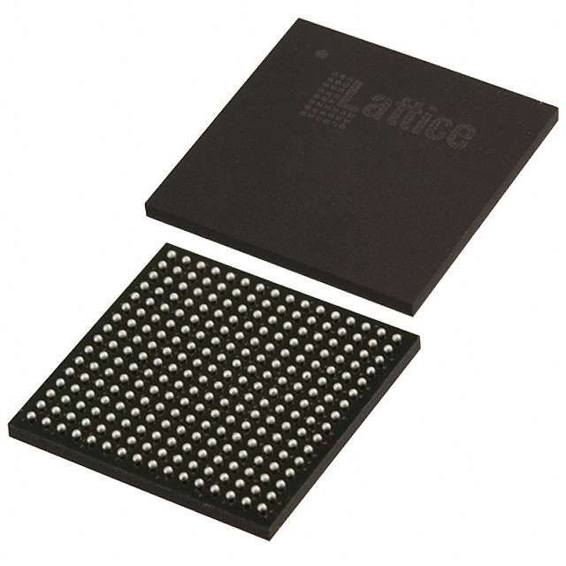
LCMXO2-7000HE-4FTG256C

Why Choose Us?
Professional Platform
B2B & B2C purchasingDelivery at full speed
1-2 days deliveryWide variety
Original manufacturers365 days guarantee
Responsible quality
.png)


Tech Specifications
LCMXO2-7000HE-4FTG256C Description
The LCMXO2-7000HE-4FTG256C is a high-performance field programmable gate array (FPGA) from Lattice Semiconductor. This device is designed to provide high-speed and low-power performance, making it suitable for a wide range of applications.
Description:
The LCMXO2-7000HE-4FTG256C is a member of Lattice's low power, low cost, and small form factor ECP5 FPGA family. It features a high-performance 28 nm process technology and a compact 256-pin flip-chip ball grid array (FCBGA) package. This device is designed for applications that require low power consumption, high-speed performance, and small form factor.
Features:
- 28 nm process technology for high-speed and low-power performance
- Compact 256-pin flip-chip ball grid array (FCBGA) package
- Wide range of I/O options for flexible system integration
- Advanced DSP blocks for high-speed data processing
- Integrated security features for enhanced system protection
- Low power consumption for extended battery life in portable applications
- Support for a variety of communication protocols, including Ethernet, PCIe, and USB
Applications:
The LCMXO2-7000HE-4FTG256C is suitable for a wide range of applications, including:
- Communications infrastructure, such as 5G base stations and optical transport networks
- Industrial automation and control systems, including motor control and sensor fusion
- Consumer electronics, such as smart home devices and wearables
- Automotive applications, including advanced driver assistance systems (ADAS) and infotainment systems
- Aerospace and defense applications, including radar and electronic warfare systems
- High-performance computing, including data center acceleration and edge computing
In summary, the LCMXO2-7000HE-4FTG256C is a versatile FPGA that offers high-speed performance, low power consumption, and a compact form factor. Its wide range of features and applications make it an excellent choice for a variety of high-performance and low-power applications.
FAQ
Not available to buy online? Want the lower wholesale price? Please Send RFQ to get best price, we will respond immediately


.png?x-oss-process=image/format,webp/resize,h_32)


