

Lattice Semiconductor
LCMXO256C-3MN100C
FPGAs

Not available to buy online? Want the lower wholesale price? Please Send RFQ to get best price, we will respond immediately


.png?x-oss-process=image/format,webp/resize,p_30)


LCMXO256C-3MN100C Description
Lattice Semiconductor's LCMXO256C-3MN100C is a high-performance field programmable gate array (FPGA) that offers a range of features and applications for various industries.
Description:
The LCMXO256C-3MN100C is a member of Lattice's MachXO2 family of low power FPGAs. It is a compact, 256-macrocell device that is designed for use in a wide range of applications, including automotive, consumer, industrial, and medical electronics.
Features:
- Low power consumption: The LCMXO256C-3MN100C is designed to operate at low power levels, making it ideal for battery-powered and energy-sensitive applications.
- High performance: The device offers high-speed performance and a wide range of I/O options, making it suitable for demanding applications that require fast data processing and communication.
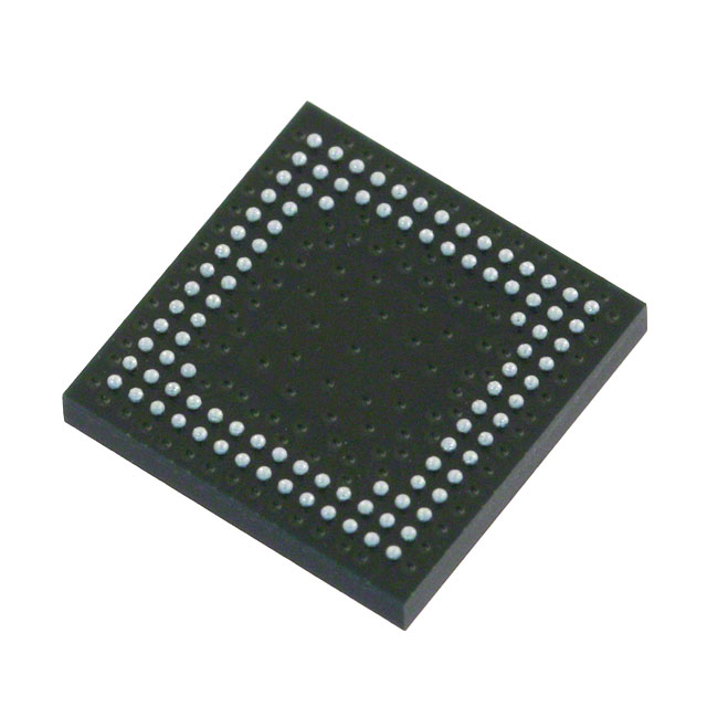
- Small form factor: The LCMXO256C-3MN100C is available in a compact 100-ball fine-pitch ball grid array (FBGA) package, making it suitable for space-constrained applications.
- Versatile I/O options: The device provides a range of I/O options, including LVCMOS, 1.2V, 1.5V, 1.8V, 2.5V, and 3.3V, allowing it to interface with various external components and systems.
- Security features: The LCMXO256C-3MN100C includes security features such as secure bitstream encryption and user-controlled configuration access, ensuring the protection of intellectual property and system integrity.
Applications:
- Automotive: The LCMXO256C-3MN100C can be used in various automotive applications, including infotainment systems, advanced driver assistance systems (ADAS), and body control modules.
- Consumer electronics: The device is suitable for use in consumer electronics such as smartphones, tablets, and wearable devices, where low power consumption and high performance are critical.
- Industrial control: The LCMXO256C-3MN100C can be used in industrial control systems for motor control, sensor interfacing, and data acquisition.
- Medical electronics: The device is suitable for use in medical electronics, such as patient monitoring systems, imaging equipment, and diagnostic devices, where reliability and security are essential.
- Communications: The LCMXO256C-3MN100C can be used in communication systems, such as base stations, routers, and switches, where high-speed data processing and communication are required.
In summary, Lattice Semiconductor's LCMXO256C-3MN100C is a versatile, low-power FPGA that offers a range of features and applications for various industries, including automotive, consumer electronics, industrial control, medical electronics, and communications. Its compact form factor, low power consumption, and high performance make it an ideal choice for a wide range of applications.
Tech Specifications
LCMXO256C-3MN100C Documents
Download datasheets and manufacturer documentation for LCMXO256C-3MN100C
Alternate Assembly Revision B 17/Nov/2014 LCMXO_MachXO Family Datasheet Product Selector Guide All Dev Pkg Mark Chg 12/Nov/2018 LCMXO_MachXO Family Datasheet Multiple Devices Cu Wire 01/Jul/2013 Top Mark Format Change 20/Dec/2023 Related Parts


Relevant Search
Shopping Guide


.png?x-oss-process=image/format,webp/resize,h_32)


©2025 ERSA Electronics Corporation.