

Lattice Semiconductor
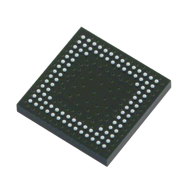
LCMXO256C-5MN100C
FPGAs

Not available to buy online? Want the lower wholesale price? Please Send RFQ to get best price, we will respond immediately


.png?x-oss-process=image/format,webp/resize,p_30)


LCMXO256C-5MN100C Description
The LCMXO256C-5MN100C is a high-performance, low-power FPGA (Field-Programmable Gate Array) from Lattice Semiconductor. This device is part of the LatticeMico series and is designed for a wide range of applications, including industrial, automotive, and consumer electronics.
Description:
The LCMXO256C-5MN100C is a 256-macrocell FPGA that offers a combination of high performance, low power consumption, and small form factor. It is based on Lattice's advanced low-power 5G process technology, which enables designers to achieve high performance while minimizing power consumption.
Features:
- 256 macrocells: The LCMXO256C-5MN100C provides a high level of integration and flexibility for various applications.
- Low power consumption: Lattice's 5G process technology allows for significant power savings, making it suitable for battery-powered and energy-sensitive applications.
- Small form factor: The device is available in a compact 5x5mm package, making it ideal for space-constrained designs.
- High-speed performance: The LCMXO256C-5MN100C supports high-speed I/O interfaces, making it suitable for high-speed data processing and communication applications.
- Configurable logic blocks: The device features a variety of configurable logic blocks, allowing designers to tailor the FPGA to their specific application requirements.
- Integrated memory: The LCMXO256C-5MN100C includes on-chip memory resources, providing additional flexibility for data storage and processing.
Applications:
The LCMXO256C-5MN100C is suitable for a wide range of applications, including:
- Industrial control systems: The low power consumption and high performance make it ideal for motor control, sensor interfacing, and other industrial applications.
- Automotive electronics: The device's robustness and reliability make it suitable for automotive applications such as infotainment systems, advanced driver assistance systems (ADAS), and body control modules.
- Consumer electronics: The small form factor and low power consumption make it suitable for portable devices, wearables, and smart home applications.
- Communication systems: The high-speed I/O interfaces and configurable logic blocks make the LCMXO256C-5MN100C suitable for communication systems, such as routers, switches, and base stations.
- Medical electronics: The device's low power consumption and small form factor make it suitable for battery-powered medical devices, such as portable monitoring systems and diagnostic equipment.
In summary, the LCMXO256C-5MN100C from Lattice Semiconductor is a versatile, low-power FPGA that offers a combination of high performance, small form factor, and integrated memory resources. It is suitable for a wide range of applications, including industrial control systems, automotive electronics, consumer electronics, communication systems, and medical electronics.
Tech Specifications
LCMXO256C-5MN100C Documents
Download datasheets and manufacturer documentation for LCMXO256C-5MN100C
Alternate Assembly/Test Site 14/Apr/2014 LCMXO_MachXO Family Datasheet Product Selector Guide All Dev Pkg Mark Chg 12/Nov/2018 LCMXO_MachXO Family Datasheet Multiple Devices Cu Wire 01/Jul/2013 Top Mark Format Change 20/Dec/2023 Related Parts


Relevant Search
Shopping Guide


.png?x-oss-process=image/format,webp/resize,h_32)


©2025 ERSA Electronics Corporation.