

Lattice Semiconductor
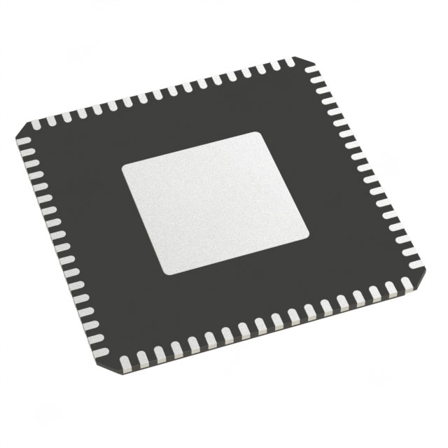
LCMXO3D-4300ZC-2SG72C
FPGAs

Not available to buy online? Want the lower wholesale price? Please Send RFQ to get best price, we will respond immediately


.png?x-oss-process=image/format,webp/resize,p_30)


LCMXO3D-4300ZC-2SG72C Description
The Lattice Semiconductor's LCMXO3D-4300ZC-2SG72C is a high-performance field programmable gate array (FPGA) device that is designed for use in a wide range of applications. This device is part of the MachXO3D family of FPGAs, which are known for their low power consumption, small form factor, and high integration.
Description:
The LCMXO3D-4300ZC-2SG72C is a high-density FPGA that features a programmable logic array, a wide range of I/O options, and a variety of on-chip resources. It is available in a compact 72-ball fine pitch ball grid array (FBGA) package, making it suitable for use in a variety of applications where space is at a premium.
Features:
- High-density programmable logic array
- Wide range of I/O options
- On-chip resources such as memory blocks, digital signal processing blocks, and phase-locked loops
- Low power consumption
- Small form factor
- Available in a 72-ball fine pitch ball grid array (FBGA) package
Applications:
The LCMXO3D-4300ZC-2SG72C is suitable for use in a wide range of applications, including:
- Industrial control systems
- Consumer electronics
- Automotive systems
- Telecommunications equipment
- Medical devices
- Aerospace and defense systems
- Internet of Things (IoT) devices
Overall, the LCMXO3D-4300ZC-2SG72C is a versatile FPGA that offers high performance, low power consumption, and a small form factor, making it an ideal choice for a wide range of applications.
Tech Specifications
LCMXO3D-4300ZC-2SG72C Documents
Download datasheets and manufacturer documentation for LCMXO3D-4300ZC-2SG72C
MachXO3D Device Family Top Mark Format Change 20/Dec/2023 Related Parts


Relevant Search
Shopping Guide


.png?x-oss-process=image/format,webp/resize,h_32)


©2025 ERSA Electronics Corporation.