
 German
 Japanese
 Portuguese
 Korea
Korea
 Mexico
 Dutch
Dutch


Lattice Semiconductor
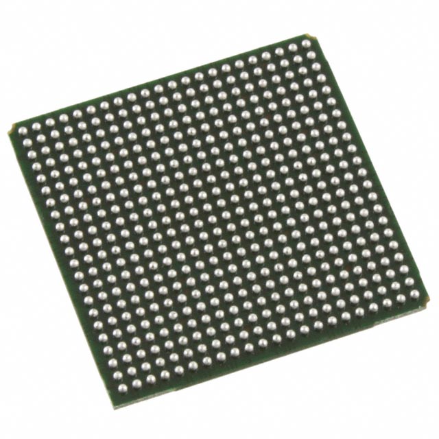
LFE2M35E-6F484C

Why Choose Us?
Professional Platform
B2B & B2C purchasingDelivery at full speed
1-2 days deliveryWide variety
Original manufacturers365 days guarantee
Responsible quality
.png)


Tech Specifications
LFE2M35E-6F484C Description
Lattice Semiconductor's LFE2M35E-6F484C is a high-performance programmable logic device designed for a wide range of applications. This device is part of Lattice's low-power, small form-factor ECP family, making it an ideal choice for space-constrained and power-sensitive systems.
Description:
The LFE2M35E-6F484C is a field-programmable gate array (FPGA) that offers a combination of high logic density, low power consumption, and small package size. It is based on Lattice's proprietary ECP (Enhanced Connectivity Platform) technology, which provides high-speed performance and advanced connectivity options.
Features:
- High Logic Density: The LFE2M35E-6F484C provides a high density of programmable logic resources, making it suitable for complex designs and applications.
- Low Power Consumption: This FPGA is designed for low-power operation, making it an excellent choice for battery-powered and energy-sensitive applications.
- Small Form-Factor: The LFE2M35E-6F484C is available in a compact 484-ball FBGA package, making it suitable for space-constrained designs.
- Enhanced Connectivity: The device features a high-speed transceiver with support for data rates up to 3.125 Gbps, as well as a range of I/O options for flexible system integration.
- Versatile I/O Options: The LFE2M35E-6F484C offers a wide range of I/O standards, including LVCMOS, LVDS, and others, to support various interface requirements.
- On-chip Memory: The FPGA includes embedded memory resources, such as block RAM and distributed RAM, to support data storage and processing tasks.
- Security Features: The device provides security features, such as encryption and secure boot, to protect intellectual property and system integrity.
Applications:
The LFE2M35E-6F484C is suitable for a wide range of applications, including but not limited to:
- Industrial Automation: The device's low power consumption and small form-factor make it ideal for use in industrial control systems and automation equipment.
- Consumer Electronics: The FPGA's high logic density and versatile I/O options make it suitable for use in consumer electronics, such as smartphones, tablets, and wearable devices.
- Networking and Communications: The high-speed transceiver and advanced connectivity options make the LFE2M35E-6F484C suitable for networking and communication applications, such as routers, switches, and base stations.
- Automotive: The device's low power consumption and robust performance make it suitable for use in automotive applications, such as infotainment systems and advanced driver assistance systems (ADAS).
- Medical Electronics: The FPGA's small form-factor and low power consumption make it suitable for use in medical devices, such as portable diagnostic equipment and wearable health monitors.
- Aerospace and Defense: The LFE2M35E-6F484C's high performance and security features make it suitable for use in aerospace and defense applications, such as satellite communication systems and secure communication equipment.
FAQ
Not available to buy online? Want the lower wholesale price? Please Send RFQ to get best price, we will respond immediately


.png?x-oss-process=image/format,webp/resize,h_32)


