

Lattice Semiconductor
LFD2NX-17-8MG121I
FPGAs

Not available to buy online? Want the lower wholesale price? Please Send RFQ to get best price, we will respond immediately


.png?x-oss-process=image/format,webp/resize,p_30)


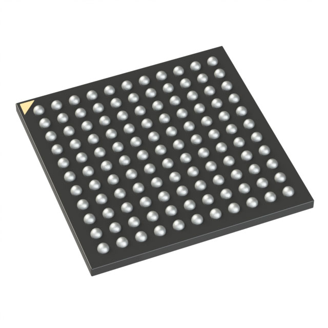
LFD2NX-17-8MG121I Description
Lattice Semiconductor's LFD2NX-17-8MG121I is a high-performance programmable logic device designed for a wide range of applications. This device is part of Lattice's low-power, small form-factor FPGA (Field-Programmable Gate Array) family, making it an ideal choice for power-sensitive and space-constrained environments.
Description:
The LFD2NX-17-8MG121I is a 17-nanometer FPGA that offers a balance of power efficiency, performance, and functionality. It is available in a compact 8x8 mm package, making it suitable for applications where board space is limited.
Features:
- Advanced 17-nanometer manufacturing process: This process technology enables lower power consumption and higher performance compared to older process nodes.
- Low power consumption: The device is designed to minimize power usage, making it ideal for battery-powered or energy-sensitive applications.
- Small form factor: The compact 8x8 mm package allows for easy integration into space-constrained designs.
- Versatile I/O options: The LFD2NX-17-8MG121I provides a range of I/O options, including LVCMOS, LVDS, and others, to support various interface requirements.
- On-chip memory: The device includes a variety of memory resources, such as block RAM and DSP slices, to support complex data processing tasks.
- Security features: The LFD2NX-17-8MG121I includes built-in security features to protect intellectual property and ensure data integrity.
- Development tools: Lattice provides a comprehensive set of development tools, including Lattice Diamond software, to facilitate design, simulation, and debugging.
Applications:
The LFD2NX-17-8MG121I is suitable for a wide range of applications, including:
- Industrial control systems: Its low power consumption and small form factor make it ideal for use in industrial automation and control applications.
- Consumer electronics: The device's compact size and low power consumption make it suitable for use in battery-powered consumer devices, such as wearables and portable gadgets.
- Automotive: The LFD2NX-17-8MG121I can be used in various automotive applications, such as infotainment systems, advanced driver assistance systems (ADAS), and body control modules.
- IoT devices: The device's low power consumption and small form factor make it well-suited for Internet of Things (IoT) devices, such as smart home appliances and sensors.
- Communications infrastructure: The versatile I/O options and on-chip memory resources make the LFD2NX-17-8MG121I suitable for use in communication infrastructure equipment, such as routers and switches.
- Medical devices: The device's low power consumption and small form factor make it suitable for use in battery-powered medical devices, such as portable monitoring equipment and diagnostic tools.
Tech Specifications
LFD2NX-17-8MG121I Documents
Download datasheets and manufacturer documentation for LFD2NX-17-8MG121I
Certus-NX Family Top Mark Format Change 20/Dec/2023 Related Parts


Relevant Search
Shopping Guide


.png?x-oss-process=image/format,webp/resize,h_32)


©2025 ERSA Electronics Corporation.