

Lattice Semiconductor
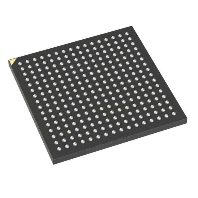
LFD2NX-40-7BG256I
FPGAs

Not available to buy online? Want the lower wholesale price? Please Send RFQ to get best price, we will respond immediately


.png?x-oss-process=image/format,webp/resize,p_30)


LFD2NX-40-7BG256I Description
Lattice Semiconductor's LFD2NX-40-7BG256I is a high-performance Field Programmable Gate Array (FPGA) that offers a range of features and applications for various industries.
Description:
The LFD2NX-40-7BG256I is a member of Lattice Semiconductor's low-power, mid-range FPGA family. It is based on the company's advanced 40nm process technology and features a compact 7x7mm ball grid array (BGA) package. This FPGA is designed to provide high performance, low power consumption, and a wide range of configurable logic resources to meet the demands of various applications.
Features:
- 40nm low-power process technology: The LFD2NX-40-7BG256I is manufactured using Lattice's advanced 40nm process technology, which enables low power consumption and high performance.
- Compact 7x7mm BGA package: The device is available in a compact 7x7mm ball grid array package, making it suitable for space-constrained applications.
- Configurable logic resources: The LFD2NX-40-7BG256I offers a wide range of configurable logic resources, including digital logic blocks, memory blocks, and dedicated logic elements, allowing for flexible and customizable designs.
- Integrated RAM and ROM: The FPGA includes integrated RAM and ROM blocks, providing additional memory resources for data storage and processing.
- High-speed I/O: The device features high-speed I/O interfaces, supporting data rates up to 1.25 Gbps, enabling fast communication with external devices.
- Security features: The LFD2NX-40-7BG256I includes advanced security features, such as encryption and authentication, to protect sensitive data and intellectual property.
- Development tools: Lattice Semiconductor provides a comprehensive set of development tools, including software development kits, integrated development environments, and IP cores, to facilitate the design and implementation of custom applications.
Applications:
The LFD2NX-40-7BG256I is suitable for a wide range of applications across various industries, including:
- Industrial automation: The FPGA can be used in industrial control systems, machine vision, and motor control applications, providing real-time processing and control capabilities.
- Consumer electronics: The device can be employed in consumer electronics, such as set-top boxes, gaming consoles, and smart home devices, for high-performance processing and connectivity.
- Automotive: The LFD2NX-40-7BG256I can be used in automotive applications, such as infotainment systems, advanced driver assistance systems (ADAS), and in-vehicle networking, offering robust performance and reliability.
- Communications: The FPGA is suitable for communication systems, including base stations, routers, and switches, providing high-speed data processing and networking capabilities.
- Aerospace and defense: The device can be used in aerospace and defense applications, such as satellite communications, radar systems, and secure communication systems, due to its advanced security features and high reliability.
In summary, Lattice Semiconductor's LFD2NX-40-7BG256I is a versatile and powerful FPGA that offers a range of features and applications for various industries. Its compact form factor, low power consumption, and advanced security features make it an ideal choice for a wide range of applications, from industrial automation to aerospace and defense.
Tech Specifications
LFD2NX-40-7BG256I Documents
Download datasheets and manufacturer documentation for LFD2NX-40-7BG256I
Certus-NX Family Preliminary~ Top Mark Format Change 20/Dec/2023 FPGA 9-26-22 Related Parts


Relevant Search
Shopping Guide


.png?x-oss-process=image/format,webp/resize,h_32)


©2025 ERSA Electronics Corporation.