

Lattice Semiconductor
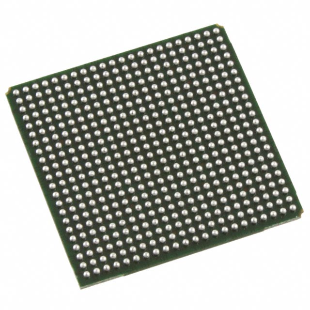
LFE2-12E-6F484C
FPGAs

Not available to buy online? Want the lower wholesale price? Please Send RFQ to get best price, we will respond immediately


.png?x-oss-process=image/format,webp/resize,p_30)


LFE2-12E-6F484C Description
Lattice Semiconductor's LFE2-12E-6F484C is a high-performance field programmable gate array (FPGA) device that offers a wide range of features and applications. Here's a description of the LFE2-12E-6F484C model:
Description:
The LFE2-12E-6F484C is a member of Lattice Semiconductor's EC family of FPGAs. It is a mid-range device that provides a balance between performance, power consumption, and cost. The device is based on Lattice's low-power, small-footprint 12 nm process technology, making it an ideal choice for a variety of applications that require high performance and low power consumption.
Features:
- Low Power Consumption: The LFE2-12E-6F484C is designed to consume low power, making it suitable for battery-operated and energy-sensitive applications.
- High Performance: The device offers high performance with its 12 nm process technology, allowing for faster processing and improved overall system performance.
- Small Form Factor: The LFE2-12E-6F484C has a compact form factor, making it ideal for space-constrained applications.
- Versatile I/O Options: The device provides a wide range of I/O options, including LVDS, DDR, and SerDes, allowing for easy integration with various peripherals and interfaces.
- Security Features: The LFE2-12E-6F484C includes advanced security features, such as encryption and authentication, to protect sensitive data and intellectual property.
- On-chip Memory: The device offers a range of on-chip memory options, including block RAM and distributed RAM, to support various memory-intensive applications.
- Configurable Logic Blocks: The LFE2-12E-6F484C features configurable logic blocks that can be programmed to perform a wide range of logic functions, making it highly versatile for various applications.
Applications:
The LFE2-12E-6F484C is suitable for a wide range of applications, including:
- Industrial Automation: The device's low power consumption and high performance make it ideal for industrial automation systems, such as motor control, sensor interfacing, and data acquisition.
- Consumer Electronics: The compact form factor and versatile I/O options make the LFE2-12E-6F484C suitable for consumer electronics, such as wearable devices, smart home appliances, and portable media players.
- Automotive: The device's robustness and reliability make it suitable for automotive applications, such as infotainment systems, advanced driver assistance systems (ADAS), and body control modules.
- Communication Systems: The LFE2-12E-6F484C's SerDes and DDR interfaces make it ideal for communication systems, such as base stations, routers, and switches.
- Security and Surveillance: The device's advanced security features and high performance make it suitable for security and surveillance applications, such as video analytics, access control, and intrusion detection systems.
- Medical Devices: The LFE2-12E-6F484C's low power consumption and small form factor make it suitable for medical devices, such as portable diagnostic equipment, patient monitoring systems, and wearable health monitors.
In summary, Lattice Semiconductor's LFE2-12E-6F484C is a versatile and high-performance FPGA device that offers a range of features and applications, making it an ideal choice for various industries and applications that require a balance between performance, power consumption, and cost.
Tech Specifications
LFE2-12E-6F484C Documents
Download datasheets and manufacturer documentation for LFE2-12E-6F484C
Alternate Qualified Test Site 30/Sep/2013 ECP2(M) Family Handbook ECP2(M) Family Product Selector Guide All Dev Pkg Mark Chg 12/Nov/2018 Tin/Lead Devices 23/Jun/2015 ECP2(M) Family Top Mark Format Change 20/Dec/2023 Related Parts


Relevant Search
Shopping Guide


.png?x-oss-process=image/format,webp/resize,h_32)


©2025 ERSA Electronics Corporation.