
 German
 Japanese
 Portuguese
 Korea
Korea
 Mexico
 Dutch
Dutch


Lattice Semiconductor
LFXP2-17E-5FTN256I

Why Choose Us?
Professional Platform
B2B & B2C purchasingDelivery at full speed
1-2 days deliveryWide variety
Original manufacturers365 days guarantee
Responsible quality
.png)


Tech Specifications
LFXP2-17E-5FTN256I Description
LFXP2-17E-5FTN256I Description
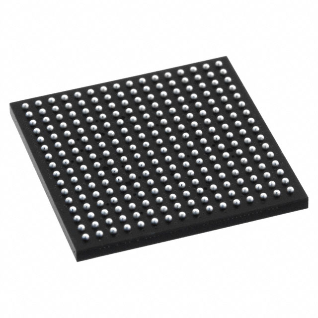
The LFXP2-17E-5FTN256I is a high-performance Field Programmable Gate Array (FPGA) from Lattice Semiconductor Corporation, designed to meet the demanding requirements of modern embedded systems. This IC is part of the XP2 series, known for its robust architecture and extensive feature set. The LFXP2-17E-5FTN256I is housed in a 256-pin Fine-Pitch Ball Grid Array (FTBGA) package, making it suitable for surface-mount applications. It operates within a voltage range of 1.14V to 1.26V, ensuring compatibility with various power supply configurations.
LFXP2-17E-5FTN256I Features
- Logic Elements and Cells: The LFXP2-17E-5FTN256I boasts 17,000 logic elements and 2,125 Logic Array Blocks (LABs) or Configurable Logic Blocks (CLBs), providing ample resources for complex digital designs.
- RAM Capacity: With a total of 282,624 RAM bits, this FPGA offers significant memory for data storage and processing tasks.
- I/O Capability: The device features 201 I/O pins, enabling extensive connectivity options for interfacing with other components and systems.
- Programmability: While the DigiKey programmability status is not verified, the LFXP2-17E-5FTN256I is designed for high flexibility, allowing users to customize the FPGA to meet specific application requirements.
- Compliance and Standards: The LFXP2-17E-5FTN256I adheres to stringent industry standards, including REACH and RoHS3 compliance, ensuring environmental sustainability and regulatory adherence. It also has a Moisture Sensitivity Level (MSL) of 3, making it suitable for a variety of manufacturing processes.
- Packaging: The device is packaged in a tray, facilitating easy handling and integration into production lines.
LFXP2-17E-5FTN256I Applications
The LFXP2-17E-5FTN256I is ideal for a wide range of applications, particularly those requiring high performance and extensive I/O capabilities. Key applications include:
- Embedded Systems: The FPGA's high logic capacity and I/O count make it suitable for complex embedded systems, such as industrial control units, automotive electronics, and medical devices.
- Digital Signal Processing (DSP): The substantial RAM and logic resources enable efficient processing of digital signals, making it ideal for applications in telecommunications, audio processing, and radar systems.
- Data Acquisition and Control: The device's robust I/O capabilities facilitate data acquisition and control tasks, making it a strong candidate for use in smart sensors, IoT devices, and automation systems.
- High-Speed Communication: The LFXP2-17E-5FTN256I's performance characteristics and extensive I/O make it well-suited for high-speed communication protocols and interfaces, such as Ethernet and USB.
Conclusion of LFXP2-17E-5FTN256I
The LFXP2-17E-5FTN256I from Lattice Semiconductor is a versatile and powerful FPGA designed to meet the needs of modern embedded systems. Its extensive logic and memory resources, coupled with a high I/O count, make it an excellent choice for a variety of applications. The device's compliance with industry standards and its surface-mount package further enhance its suitability for a wide range of manufacturing processes. Whether used in embedded systems, digital signal processing, or high-speed communication, the LFXP2-17E-5FTN256I offers a reliable and efficient solution for engineers and designers in the electronics industry.
FAQ
Not available to buy online? Want the lower wholesale price? Please Send RFQ to get best price, we will respond immediately


.png?x-oss-process=image/format,webp/resize,h_32)


