

Lattice Semiconductor
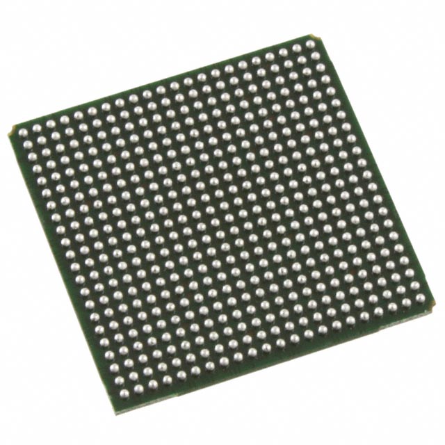
LFE2M35E-7FN484C
FPGAs

Not available to buy online? Want the lower wholesale price? Please Send RFQ to get best price, we will respond immediately


.png?x-oss-process=image/format,webp/resize,p_30)


LFE2M35E-7FN484C Description
Lattice Semiconductor's LFE2M35E-7FN484C is a high-performance programmable logic device that offers a range of features and applications for various industries. Here is a description of the LFE2M35E-7FN484C model, including its features and applications:
Description:
The LFE2M35E-7FN484C is a member of Lattice Semiconductor's family of low-cost, small form factor FPGAs (Field-Programmable Gate Arrays). This device is designed to provide a flexible and customizable solution for a wide range of applications, including automotive, industrial, and consumer electronics.
Features:
- FPGA Architecture: The LFE2M35E-7FN484C is based on Lattice's proprietary low-power FPGA architecture, which is optimized for power efficiency and performance.
- I/O Count: This device features a total of 484 I/O (input/output) pins, providing ample connectivity options for various peripherals and interfaces.
- Package Type: The LFE2M35E-7FN484C is available in a 7x8 mm Fine-Pitch Ball Grid Array (FBGA) package, which is compact and suitable for space-constrained applications.
- Operating Temperature Range: This FPGA can operate in a wide temperature range of -40°C to +125°C, making it suitable for harsh environments.
- Power Consumption: The LFE2M35E-7FN484C is designed for low power consumption, which is crucial for battery-powered and energy-sensitive applications.
- Security Features: The device includes built-in security features to protect intellectual property and ensure the integrity of the design.
- Development Tools: Lattice provides a comprehensive set of development tools, including software and hardware, to facilitate the design, simulation, and debugging of the LFE2M35E-7FN484C.
Applications:
- Automotive: The LFE2M35E-7FN484C can be used in various automotive applications, such as infotainment systems, advanced driver assistance systems (ADAS), and body control modules.
- Industrial: This FPGA is suitable for industrial applications that require real-time processing, such as motor control, robotics, and machine vision systems.
- Consumer Electronics: The LFE2M35E-7FN484C can be used in consumer electronics products, such as smart home devices, wearables, and portable gadgets.
- Communication Systems: The device can be employed in communication systems, including base stations, routers, and switches, for efficient data processing and routing.
- Medical Devices: The LFE2M35E-7FN484C can be utilized in medical devices for signal processing, image processing, and data acquisition.
In summary, Lattice Semiconductor's LFE2M35E-7FN484C is a versatile and powerful FPGA that offers a range of features suitable for various applications across different industries. Its compact form factor, low power consumption, and extensive I/O options make it an ideal choice for designers looking for a customizable and efficient solution.
Tech Specifications
LFE2M35E-7FN484C Documents
Download datasheets and manufacturer documentation for LFE2M35E-7FN484C
Alternate Qualified Test Site 30/Sep/2013 ECP2(M) Family Handbook ECP2(M) Family Product Selector Guide All Dev Pkg Mark Chg 12/Nov/2018 ECP2(M) Family Multiple Devices Cu Wire 01/Jul/2013 Top Mark Format Change 20/Dec/2023 Related Parts


Relevant Search
Shopping Guide


.png?x-oss-process=image/format,webp/resize,h_32)


©2025 ERSA Electronics Corporation.