

Lattice Semiconductor
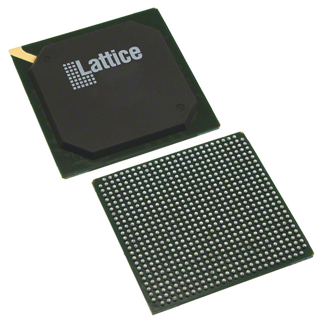
LFE3-70E-6FN672C
FPGAs

Not available to buy online? Want the lower wholesale price? Please Send RFQ to get best price, we will respond immediately


.png?x-oss-process=image/format,webp/resize,p_30)


LFE3-70E-6FN672C Description
Lattice Semiconductor's LFE3-70E-6FN672C is a high-performance programmable logic device designed for a wide range of applications. This device is part of the LatticeECP3 family, which is known for its low power consumption, high performance, and small form factor.
Description:
The LFE3-70E-6FN672C is a 6mm x 7mm fine-pitch ball grid array (FBGA) package that contains a programmable logic device with a high-density architecture. It features a large number of configurable logic elements, digital signal processing blocks, and memory resources, making it suitable for a variety of applications.
Features:
- Low power consumption: The LFE3-70E-6FN672C is designed to operate with low power consumption, making it ideal for battery-powered or energy-sensitive applications.
- High performance: With a high-density architecture and a wide range of configurable resources, the LFE3-70E-6FN672C can handle complex tasks and demanding applications.
- Small form factor: The 6mm x 7mm FBGA package allows for compact and space-efficient designs, making it suitable for portable or constrained environments.
- Versatile I/O options: The device offers a wide range of I/O options, including LVCMOS, LVDS, and serdes, providing flexibility in interfacing with other components and systems.
- Configurable logic elements: The LFE3-70E-6FN672C features a large number of configurable logic elements, allowing for custom designs and optimizations based on specific application requirements.
- Digital signal processing blocks: The device includes digital signal processing blocks that can be used for tasks such as filtering, modulation, and demodulation in communication systems.
- Memory resources: The LFE3-70E-6FN672C provides a variety of memory resources, including block RAM and distributed RAM, to support data storage and processing needs.
Applications:
The LFE3-70E-6FN672C is suitable for a wide range of applications, including but not limited to:
- Communication systems: The device can be used in communication systems for tasks such as signal processing, modulation, and demodulation.
- Industrial control: The LFE3-70E-6FN672C can be used in industrial control applications for tasks such as motor control, sensor interfacing, and data acquisition.
- Consumer electronics: The low power consumption and small form factor make it suitable for portable consumer electronics, such as wearable devices and mobile gadgets.
- Automotive: The device can be used in automotive applications for tasks such as infotainment systems, driver assistance systems, and sensor processing.
- Medical devices: The LFE3-70E-6FN672C can be used in medical devices for tasks such as signal processing, data acquisition, and control in imaging systems, monitoring devices, and diagnostic equipment.
In summary, Lattice Semiconductor's LFE3-70E-6FN672C is a versatile and high-performance programmable logic device that offers low power consumption, a small form factor, and a wide range of configurable resources. It is suitable for various applications, including communication systems, industrial control, consumer electronics, automotive, and medical devices.
Tech Specifications
LFE3-70E-6FN672C Documents
Download datasheets and manufacturer documentation for LFE3-70E-6FN672C
ECP3 Family DataSheet V1.6 All Dev Pkg Mark Chg 12/Nov/2018 Solving Intellegence, Vision, Connectivity Challenges at the Edge with ECP5 FPGAs ECP3 Family DataSheet V1.6 Top Mark Format Change 20/Dec/2023 Related Parts


Relevant Search
Shopping Guide


.png?x-oss-process=image/format,webp/resize,h_32)


©2025 ERSA Electronics Corporation.