
 German
 Japanese
 Portuguese
 Korea
Korea
 Mexico
 Dutch
Dutch


Lattice Semiconductor
LCMXO2-640HC-6TG100C

Why Choose Us?
Professional Platform
B2B & B2C purchasingDelivery at full speed
1-2 days deliveryWide variety
Original manufacturers365 days guarantee
Responsible quality
.png)


Tech Specifications
LCMXO2-640HC-6TG100C Description
The LCMXO2-640HC-6TG100C is a field programmable gate array (FPGA) from Lattice Semiconductor, a leading manufacturer of programmable logic devices. This specific model is part of the MachXO2 family, which is known for its low power consumption, small form factor, and high performance.
Description:
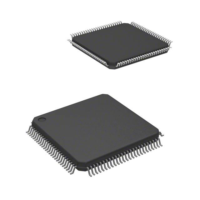
The LCMXO2-640HC-6TG100C is a high-performance, low power FPGA that is ideal for a wide range of applications. It features a 6-layer thin quad flat package (TQFP) with a total of 100 pins. The device has a programmable logic array size of 640 macrocells, which provides a good balance between logic density and I/O capabilities.
Features:
- Low Power Consumption: The MachXO2 family is designed to provide low power consumption, making it suitable for battery-powered or energy-sensitive applications.
- Small Form Factor: The 6-layer TQFP package is compact, allowing for easy integration into a variety of products.
- High Performance: The LCMXO2-640HC-6TG100C offers high-speed performance, with a maximum clock frequency of up to 400 MHz.
- Versatile I/O: The device provides a wide range of I/O options, including LVCMOS, LVDS, and SSTL, making it suitable for various interface requirements.
- Security Features: The MachXO2 family includes security features such as anti-fuse and flash-based encryption to protect intellectual property and ensure device authenticity.
- Configuration Memory: The device comes with 8 Mbit of configuration memory, providing ample space for storing the FPGA configuration.
Applications:
The LCMXO2-640HC-6TG100C is suitable for a wide range of applications, including:
- Industrial Control Systems: The device's low power consumption and high performance make it ideal for use in industrial control systems, such as motor control and sensor data processing.
- Consumer Electronics: The small form factor and low power consumption make it suitable for use in portable consumer devices, such as fitness trackers and smart home devices.
- Automotive Applications: The device's versatility and reliability make it suitable for use in automotive applications, such as infotainment systems and advanced driver assistance systems (ADAS).
- Communication Systems: The LCMXO2-640HC-6TG100C can be used in communication systems for data processing and interfacing with various communication protocols.
- Medical Devices: The device's small size and low power consumption make it suitable for use in battery-powered medical devices, such as portable monitoring systems and diagnostic equipment.
In summary, the LCMXO2-640HC-6TG100C is a versatile and high-performance FPGA that offers low power consumption, a small form factor, and a wide range of I/O options. It is suitable for a variety of applications, including industrial control systems, consumer electronics, automotive applications, communication systems, and medical devices.
FAQ
Not available to buy online? Want the lower wholesale price? Please Send RFQ to get best price, we will respond immediately


.png?x-oss-process=image/format,webp/resize,h_32)


