
 German
 Japanese
 Portuguese
 Korea
Korea
 Mexico
 Dutch
Dutch


Lattice Semiconductor
LFXP2-40E-7FN672C

Why Choose Us?
Professional Platform
B2B & B2C purchasingDelivery at full speed
1-2 days deliveryWide variety
Original manufacturers365 days guarantee
Responsible quality
.png)


Tech Specifications
LFXP2-40E-7FN672C Description
Lattice Semiconductor's LFXP2-40E-7FN672C is a high-performance programmable logic device that offers a wide range of features and applications. It is based on the company's advanced low-power FPGA technology, making it an ideal solution for a variety of applications that require high performance, low power consumption, and small form factor.
Description:
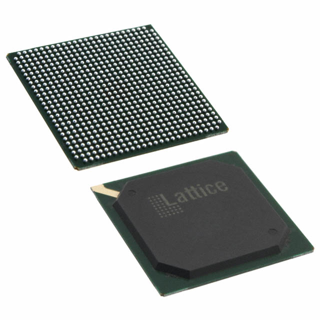
The LFXP2-40E-7FN672C is a field-programmable gate array (FPGA) that belongs to Lattice Semiconductor's low-power ECP2 series. It is available in a 7x7 mm fine-pitch ball grid array (FBGA) package and features a high-density architecture that provides up to 40,000 logic elements (LEs) and 1,200 digital signal processing (DSP) slices.
Features:
- Low Power Consumption: The LFXP2-40E-7FN672C is designed for low power applications, making it an ideal choice for battery-powered devices and energy-sensitive systems.
- High Performance: With its advanced low-power FPGA technology, the LFXP2-40E-7FN672C delivers high performance and fast processing speeds, making it suitable for demanding applications.
- Small Form Factor: The 7x7 mm FBGA package allows for compact designs, making the LFXP2-40E-7FN672C suitable for space-constrained applications.
- Versatile I/O Options: The device offers a wide range of I/O options, including LVDS, DDR, and high-speed transceivers, making it suitable for various interface requirements.
- Configurable Logic: The high-density architecture provides up to 40,000 LEs and 1,200 DSP slices, allowing for flexible and customizable logic designs.
- Security Features: The LFXP2-40E-7FN672C includes built-in security features, such as encryption and authentication, to protect intellectual property and ensure secure communication.
Applications:
- Industrial Automation: The LFXP2-40E-7FN672C can be used in industrial control systems, where its low power consumption, high performance, and small form factor are advantageous.
- Consumer Electronics: The device is suitable for battery-powered consumer electronics, such as wearable devices, portable gaming consoles, and smart home devices, due to its low power consumption and compact size.
- Communication Systems: The LFXP2-40E-7FN672C can be used in communication systems, such as base stations and routers, where its high-speed transceivers and versatile I/O options are beneficial.
- Automotive: The device can be used in automotive applications, such as infotainment systems and advanced driver assistance systems (ADAS), where its low power consumption, high performance, and security features are essential.
- Medical Devices: The LFXP2-40E-7FN672C is suitable for medical devices, such as portable diagnostic equipment and monitoring systems, where its small form factor, low power consumption, and security features are important.
In summary, Lattice Semiconductor's LFXP2-40E-7FN672C is a versatile, low-power FPGA that offers a range of features and applications, making it an ideal solution for various industries and applications that require high performance, low power consumption, and compact designs.
FAQ
Not available to buy online? Want the lower wholesale price? Please Send RFQ to get best price, we will respond immediately


.png?x-oss-process=image/format,webp/resize,h_32)


