
 German
 Japanese
 Portuguese
 Korea
Korea
 Mexico
 Dutch
Dutch


Lattice Semiconductor
LFEC15E-3FN484C

Why Choose Us?
Professional Platform
B2B & B2C purchasingDelivery at full speed
1-2 days deliveryWide variety
Original manufacturers365 days guarantee
Responsible quality
.png)


Tech Specifications
LFEC15E-3FN484C Description
LFEC15E-3FN484C Description
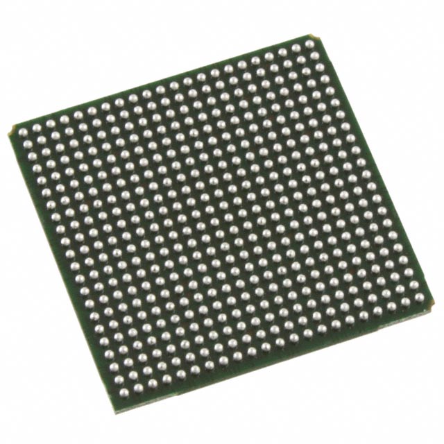
The LFEC15E-3FN484C is an IC FPGA from Lattice Semiconductor Corporation, part of the EC series. This device is designed for high-performance applications requiring extensive logic capabilities and a large number of I/O connections. It features 15,400 logic elements/cells and 352 I/Os, making it suitable for complex digital designs. The operating temperature range of 0°C to 85°C (TJ) ensures reliable performance in a variety of environmental conditions. The LFEC15E-3FN484C is housed in a 484FBGA package, which is ideal for surface mount applications, providing a compact and robust solution for embedded systems.
LFEC15E-3FN484C Features
- Logic Elements/Cells: 15,400 logic elements/cells offer extensive programmability and flexibility for complex digital designs.
- I/O Count: 352 I/Os provide ample connectivity options, making it suitable for applications requiring multiple interfaces and peripheral connections.
- Operating Temperature: A wide operating temperature range of 0°C to 85°C (TJ) ensures reliable performance in various environmental conditions.
- Supply Voltage: The device operates within a supply voltage range of 1.14V to 1.26V, providing efficient power consumption and compatibility with modern low-power systems.
- Package Type: The 484FBGA package is ideal for surface mount applications, offering a compact and robust solution for embedded systems.
- Moisture Sensitivity Level: MSL 3 (168 Hours) ensures the device remains protected during manufacturing processes, reducing the risk of moisture-related failures.
- Compliance: The LFEC15E-3FN484C is REACH unaffected and classified under HTSUS code 8542.39.0001, ensuring compliance with international regulations.
- RAM Bits: 358,400 total RAM bits provide significant onboard memory for data storage and processing, enhancing the device's capabilities for complex operations.
LFEC15E-3FN484C Applications
The LFEC15E-3FN484C is ideal for a range of high-performance applications, including:
- Telecommunications: Ideal for base station controllers, signal processing units, and other telecom equipment requiring high-speed data processing and extensive I/O connectivity.
- Industrial Automation: Suitable for programmable logic controllers (PLCs), robotic controllers, and other industrial systems that demand robust and reliable digital control.
- Consumer Electronics: Applicable in advanced consumer devices such as smart TVs, gaming consoles, and high-end multimedia systems where complex digital processing and multiple I/O interfaces are required.
- Automotive: Can be used in advanced driver-assistance systems (ADAS), infotainment systems, and other automotive electronic applications that require high-performance processing and connectivity.
Conclusion of LFEC15E-3FN484C
The LFEC15E-3FN484C from Lattice Semiconductor Corporation is a powerful and versatile IC FPGA designed for high-performance embedded systems. With its extensive logic capabilities, large number of I/O connections, and wide operating temperature range, it offers significant advantages over similar models. The device's compact 484FBGA package and low-power supply voltage make it an ideal choice for modern, space-constrained applications. Despite its obsolete status, the LFEC15E-3FN484C remains a reliable and efficient solution for a variety of demanding applications, ensuring continued performance and compatibility in the electronics industry.
FAQ
Not available to buy online? Want the lower wholesale price? Please Send RFQ to get best price, we will respond immediately


.png?x-oss-process=image/format,webp/resize,h_32)


