
 German
 Japanese
 Portuguese
 Korea
Korea
 Mexico
 Dutch
Dutch


Lattice Semiconductor
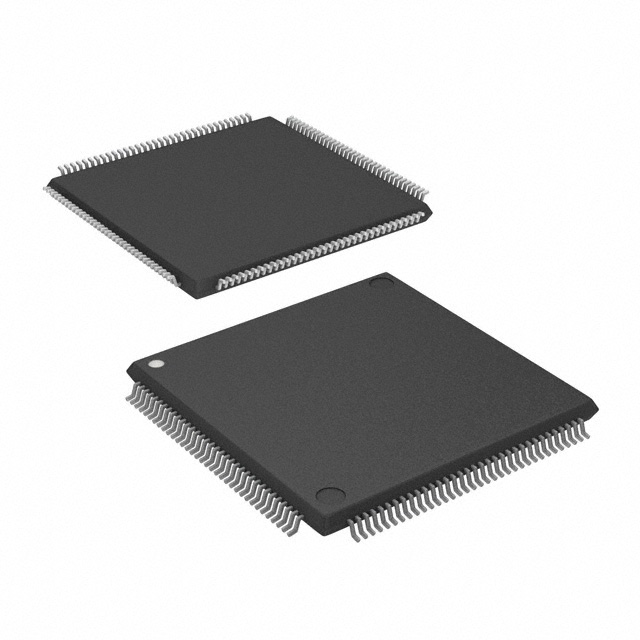
LFEC1E-3TN144C

Why Choose Us?
Professional Platform
B2B & B2C purchasingDelivery at full speed
1-2 days deliveryWide variety
Original manufacturers365 days guarantee
Responsible quality
.png)


Tech Specifications
LFEC1E-3TN144C Description
Lattice Semiconductor's LFEC1E-3TN144C is a high-performance programmable logic device that offers a wide range of features and applications. Here is a description of the LFEC1E-3TN144C model, including its features and applications:
Description:
The LFEC1E-3TN144C is a member of Lattice Semiconductor's family of FPGAs (Field-Programmable Gate Arrays). It is a low-cost, mid-range device that provides a flexible and customizable solution for various applications. The device comes in a 144-ball fine-pitch ball grid array (FBGA) package, making it suitable for use in compact and space-constrained systems.
Features:
- Low power consumption: The LFEC1E-3TN144C is designed to operate with low power consumption, making it an ideal choice for battery-powered or energy-efficient applications.
- High performance: The device offers high-speed performance, with a maximum frequency of up to 400 MHz, ensuring fast processing and quick response times.
- Versatile I/O options: The LFEC1E-3TN144C provides a wide range of I/O options, including LVCMOS, LVDS, and serdes, allowing for easy integration with various peripherals and interfaces.
- Configurable logic blocks: The device features configurable logic blocks (CLBs) that can be programmed to perform a variety of functions, providing flexibility in designing custom solutions.
- Embedded memory: The LFEC1E-3TN144C includes embedded memory resources, such as block RAM and distributed RAM, which can be used for data storage and processing tasks.
- Security features: The device offers security features, such as encryption and secure boot, to protect sensitive data and ensure the integrity of the system.
Applications:
The LFEC1E-3TN144C is suitable for a wide range of applications, including but not limited to:
- Industrial control systems: The device's low power consumption and high performance make it ideal for use in industrial control systems, where reliability and efficiency are crucial.
- Communication systems: The versatile I/O options and high-speed performance of the LFEC1E-3TN144C make it suitable for use in communication systems, such as routers, switches, and base stations.
- Consumer electronics: The compact form factor and customizable nature of the device make it an excellent choice for use in consumer electronics, such as smartphones, tablets, and smart home devices.
- Automotive systems: The LFEC1E-3TN144C can be used in various automotive applications, such as infotainment systems, driver assistance systems, and powertrain control.
- Security systems: The device's security features make it suitable for use in security systems, such as surveillance cameras, access control systems, and encryption devices.
In summary, Lattice Semiconductor's LFEC1E-3TN144C is a versatile and high-performance FPGA that offers a range of features and applications, making it an excellent choice for various industries and applications.
FAQ
Not available to buy online? Want the lower wholesale price? Please Send RFQ to get best price, we will respond immediately


.png?x-oss-process=image/format,webp/resize,h_32)


