

Lattice Semiconductor
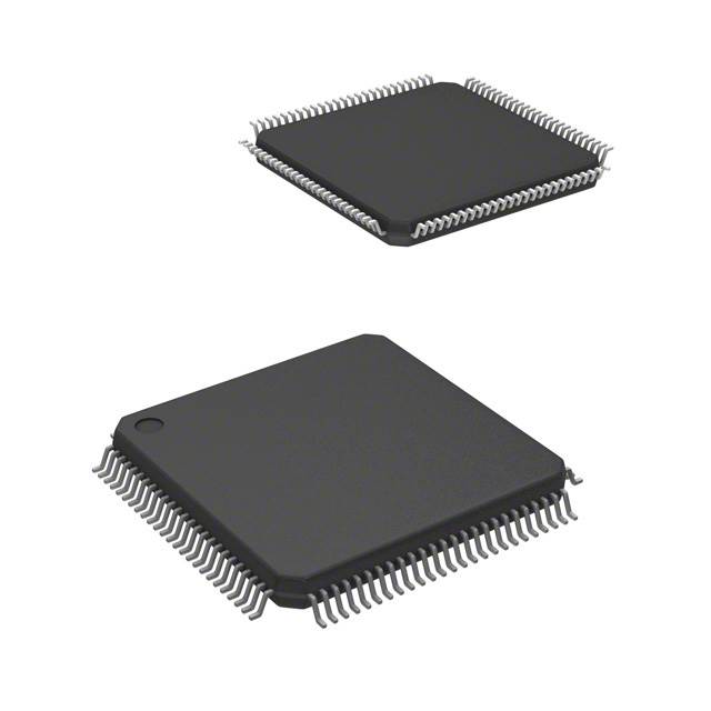
LFEC1E-3T100C
FPGAs

Not available to buy online? Want the lower wholesale price? Please Send RFQ to get best price, we will respond immediately


.png?x-oss-process=image/format,webp/resize,p_30)


LFEC1E-3T100C Description
Lattice Semiconductor's LFEC1E-3T100C is a high-performance programmable logic device designed for a wide range of applications. This device is part of Lattice's EC family of FPGAs, which are known for their low power consumption, small form factor, and high integration.
Description:
The LFEC1E-3T100C is a mid-range FPGA that offers a balance of performance, power efficiency, and cost-effectiveness. It features a compact 256-ball fine-pitch ball grid array (FBGA) package, making it suitable for space-constrained applications. The device has a maximum operating frequency of 100 MHz and provides up to 3,270 logic elements (LEs) for complex designs.
Features:
- Low power consumption: The LFEC1E-3T100C is designed for energy-efficient operation, making it ideal for battery-powered or environmentally friendly applications.
- Compact form factor: The 256-ball FBGA package allows for easy integration into small and portable devices.
- High integration: With up to 3,270 LEs, the LFEC1E-3T100C can handle complex designs and multiple functions within a single device.
- Versatile I/O options: The device supports a wide range of I/O standards, making it suitable for various interface requirements.
- Security features: The LFEC1E-3T100C includes security features such as encryption and authentication to protect intellectual property and ensure data integrity.
- Development tools: Lattice provides a comprehensive set of development tools, including design software, IP cores, and documentation, to help engineers quickly and easily develop their applications.
Applications:
The LFEC1E-3T100C is suitable for a wide range of applications, including but not limited to:
- Industrial control and automation: The device's low power consumption and high integration make it ideal for industrial applications such as motor control, sensor interfacing, and data acquisition systems.
- Consumer electronics: The compact form factor and versatile I/O options make the LFEC1E-3T100C suitable for consumer electronics such as wearable devices, smart home appliances, and portable gadgets.
- Communication systems: The device's high-speed operation and secure features make it suitable for communication systems such as base stations, routers, and switches.
- Automotive: The LFEC1E-3T100C can be used in various automotive applications, including infotainment systems, advanced driver assistance systems (ADAS), and body control modules.
- Medical devices: The device's low power consumption and security features make it suitable for medical devices such as patient monitoring systems, diagnostic equipment, and portable medical instruments.
In summary, Lattice Semiconductor's LFEC1E-3T100C is a versatile, low-power, and compact FPGA that offers a balance of performance, power efficiency, and cost-effectiveness. Its wide range of features and applications make it suitable for various industries, including industrial control, consumer electronics, communication systems, automotive, and medical devices.
Tech Specifications
LFEC1E-3T100C Documents
Download datasheets and manufacturer documentation for LFEC1E-3T100C
ECP, EC Family Package Diagrams Leaded Pkg PCB Layout Guide All Dev Pkg Mark Chg 12/Nov/2018 LatticeEC/P and LatticeXP Devices 25/Jul/2013 ECP, EC Family Top Mark Format Change 20/Dec/2023 Related Parts


Relevant Search
Shopping Guide


.png?x-oss-process=image/format,webp/resize,h_32)


©2025 ERSA Electronics Corporation.