
 German
 Japanese
 Portuguese
 Korea
Korea
 Mexico
 Dutch
Dutch


Lattice Semiconductor
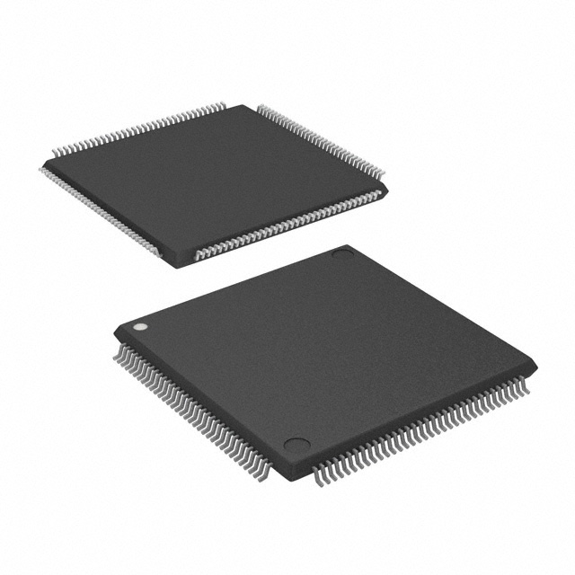
LFEC1E-4TN144C

Why Choose Us?
Professional Platform
B2B & B2C purchasingDelivery at full speed
1-2 days deliveryWide variety
Original manufacturers365 days guarantee
Responsible quality
.png)


Tech Specifications
LFEC1E-4TN144C Description
Lattice Semiconductor's LFEC1E-4TN144C is a field programmable gate array (FPGA) device that offers a versatile and customizable solution for a wide range of applications. This device is designed to provide high performance, low power consumption, and a small form factor, making it suitable for use in various industries and applications.
Description:
The LFEC1E-4TN144C is a member of Lattice Semiconductor's EC family of FPGAs. It is a mid-range device that combines the benefits of low power consumption, high performance, and small form factor. This device is based on Lattice's advanced low-power 40 nm process technology, which enables it to deliver excellent power efficiency and performance.
Features:
- Low Power Consumption: The LFEC1E-4TN144C is designed to operate with low power consumption, making it an ideal choice for battery-powered or energy-sensitive applications.
- High Performance: This FPGA device offers high performance and fast processing speeds, allowing it to handle complex tasks and demanding applications with ease.
- Small Form Factor: The LFEC1E-4TN144C has a compact form factor, making it suitable for use in space-constrained applications and systems.
- Versatility: This device is highly customizable and can be programmed to perform a wide range of functions, making it suitable for various applications.
- Security Features: The LFEC1E-4TN144C includes built-in security features to protect sensitive data and intellectual property.
- Robust Design: This FPGA device is designed to withstand harsh environmental conditions and is suitable for use in industrial and automotive applications.
Applications:
The LFEC1E-4TN144C can be used in a wide range of applications, including:
- Industrial Automation: The device's low power consumption and high performance make it suitable for use in industrial automation systems, such as motor control, robotics, and machine vision.
- Automotive: The LFEC1E-4TN144C can be used in automotive applications, such as infotainment systems, advanced driver assistance systems (ADAS), and powertrain control.
- Consumer Electronics: This FPGA device can be used in consumer electronics, such as smartphones, tablets, and wearable devices, for functions like image processing, audio processing, and connectivity.
- Telecommunications: The LFEC1E-4TN144C can be used in telecommunications infrastructure, such as base stations, routers, and switches, for functions like signal processing and data routing.
- Aerospace and Defense: This FPGA device can be used in aerospace and defense applications, such as satellite communication systems, radar systems, and secure communication devices.
In summary, Lattice Semiconductor's LFEC1E-4TN144C is a versatile and powerful FPGA device that offers low power consumption, high performance, and a small form factor. Its wide range of features and applications make it an excellent choice for various industries and applications, including industrial automation, automotive, consumer electronics, telecommunications, and aerospace and defense.
FAQ
Not available to buy online? Want the lower wholesale price? Please Send RFQ to get best price, we will respond immediately


.png?x-oss-process=image/format,webp/resize,h_32)


