

Lattice Semiconductor
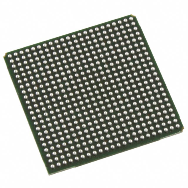
LFECP6E-4F484C
FPGAs
Not available to buy online? Want the lower wholesale price? Please Send RFQ to get best price, we will respond immediately


.png?x-oss-process=image/format,webp/resize,p_30)


LFECP6E-4F484C Description
Lattice Semiconductor's LFECP6E-4F484C is a high-performance programmable logic device designed for a wide range of applications. This device is part of the LatticeECP family, which offers a combination of flexibility, performance, and low power consumption.
Description:
The LFECP6E-4F484C is a programmable logic device that features a high-density FPGA architecture. It is built on a 6-input lookup table (LUT) based technology, which allows for efficient implementation of complex logic functions. The device has a total of 484 macrocells, making it suitable for medium-sized applications.
Features:
- High-density FPGA architecture: The LFECP6E-4F484C is based on a 6-input LUT technology, which provides a high level of integration and flexibility for various applications.
- Low power consumption: The device is designed to operate at low power levels, making it suitable for battery-powered and energy-sensitive applications.
- Versatile I/O options: The LFECP6E-4F484C offers a wide range of I/O options, including LVDS, LVCMOS, and SSTL, allowing for easy integration with various peripherals and interfaces.
- On-chip memory: The device includes on-chip memory resources, such as block RAM and distributed RAM, which can be used for data storage and processing tasks.
- High-speed performance: The LFECP6E-4F484C is capable of operating at high clock frequencies, making it suitable for applications that require fast data processing and real-time performance.
- Configurable logic blocks: The device features configurable logic blocks that can be programmed to perform a wide range of logic functions, providing flexibility for various applications.
Applications:
The LFECP6E-4F484C is suitable for a wide range of applications, including but not limited to:
- Industrial control systems: The device can be used in industrial control systems for implementing complex logic functions and interfacing with various sensors and actuators.
- Communication systems: The LFECP6E-4F484C can be used in communication systems for implementing protocols and managing data transmission.
- Consumer electronics: The device can be used in consumer electronics, such as set-top boxes and gaming consoles, for implementing complex logic functions and managing multimedia data.
- Automotive systems: The LFECP6E-4F484C can be used in automotive systems for implementing safety-critical functions and managing various electronic control units (ECUs).
- Medical devices: The device can be used in medical devices for implementing complex algorithms and managing data processing tasks.
- Networking equipment: The LFECP6E-4F484C can be used in networking equipment for implementing network protocols and managing data traffic.
In summary, the Lattice Semiconductor's LFECP6E-4F484C is a versatile and high-performance programmable logic device that offers a range of features suitable for various applications, including industrial control systems, communication systems, consumer electronics, automotive systems, medical devices, and networking equipment. Its high-density FPGA architecture, low power consumption, and flexible I/O options make it an ideal choice for designers looking for a reliable and efficient solution.
Tech Specifications
LFECP6E-4F484C Documents
Download datasheets and manufacturer documentation for LFECP6E-4F484C
 Package Diagrams All Dev Pkg Mark Chg 12/Nov/2018 LatticeEC/P and LatticeXP Devices 25/Jul/2013 Top Mark Format Change 20/Dec/2023
 Related Parts


Relevant Search
Shopping Guide


.png?x-oss-process=image/format,webp/resize,h_32)


©2025 ERSA Electronics Corporation.