
 German
 Japanese
 Portuguese
 Korea
Korea
 Mexico
 Dutch
Dutch


Lattice Semiconductor
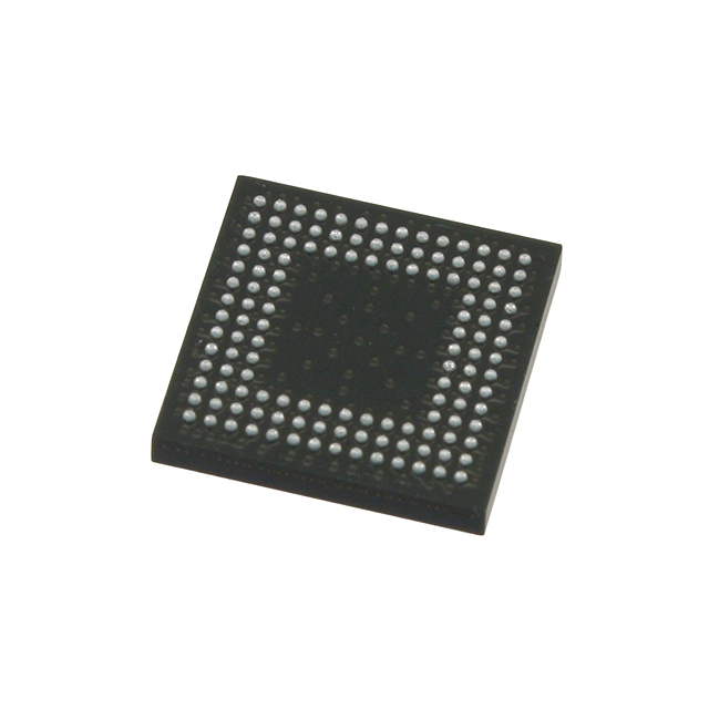
LFXP2-8E-5MN132C

Why Choose Us?
Professional Platform
B2B & B2C purchasingDelivery at full speed
1-2 days deliveryWide variety
Original manufacturers365 days guarantee
Responsible quality
.png)


Tech Specifications
LFXP2-8E-5MN132C Description
Lattice Semiconductor's LFXP2-8E-5MN132C is a high-performance programmable logic device that offers a range of features and applications for various industries.
Description:
The LFXP2-8E-5MN132C is a member of Lattice Semiconductor's low-power, small form-factor FPGA family. It is based on the company's advanced 28 nm low-power process technology, which enables high performance and low power consumption. The device is available in a compact 132-ball fine pitch ball grid array (FBGA) package, making it suitable for space-constrained applications.
Features:
- Advanced 28 nm low-power process technology for high performance and low power consumption.
- Compact 132-ball fine pitch ball grid array (FBGA) package for space-constrained applications.
- Wide range of I/O options for flexible system integration.
- Integrated security features for protection against unauthorized access and tampering.
- Support for a variety of communication protocols, including Ethernet, PCIe, and USB.
- Configurable logic elements and memory resources for customizable system design.
- On-chip debug and trace capabilities for efficient development and troubleshooting.
Applications:
The LFXP2-8E-5MN132C is suitable for a wide range of applications, including but not limited to:
- Industrial automation and control systems, where its low power consumption and small form factor are advantageous.
- Communications infrastructure, such as network routers and switches, where its support for various communication protocols is beneficial.
- Consumer electronics, such as set-top boxes and smart home devices, where its integrated security features and customizable design options are valuable.
- Automotive systems, including infotainment and advanced driver assistance systems (ADAS), where its reliability and performance are crucial.
- Aerospace and defense applications, where its on-chip debug and trace capabilities can aid in efficient development and troubleshooting.
In summary, Lattice Semiconductor's LFXP2-8E-5MN132C is a versatile and powerful FPGA that offers a range of features and applications for various industries. Its advanced process technology, compact form factor, and customizable design options make it an ideal choice for a wide range of applications.
FAQ
Not available to buy online? Want the lower wholesale price? Please Send RFQ to get best price, we will respond immediately


.png?x-oss-process=image/format,webp/resize,h_32)


