

Lattice Semiconductor
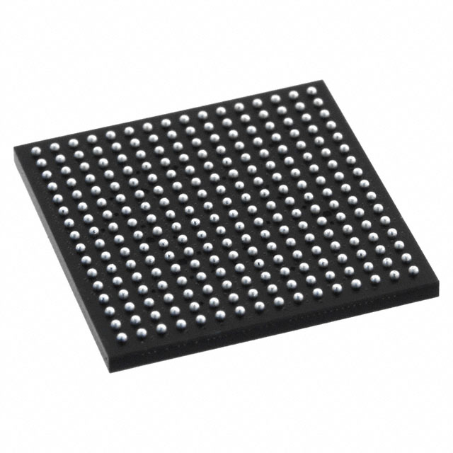
LFXP2-8E-6FTN256C
FPGAs

Not available to buy online? Want the lower wholesale price? Please Send RFQ to get best price, we will respond immediately


.png?x-oss-process=image/format,webp/resize,p_30)


LFXP2-8E-6FTN256C Description
Lattice Semiconductor's LFXP2-8E-6FTN256C is a field programmable gate array (FPGA) that offers a versatile and customizable solution for a wide range of applications. This device is designed to provide high performance, low power consumption, and a small form factor, making it suitable for a variety of electronic systems.
Description:
The LFXP2-8E-6FTN256C is a member of Lattice Semiconductor's low-cost, low-power ECP2 series of FPGAs. It features a 6-input look-up table (LUT) based architecture and is available in a 256-ball fine pitch ball grid array (FBGA) package. This device is designed for use in a wide range of applications, including communications, industrial control, consumer electronics, and more.
Features:
- 6-input LUT-based architecture for high performance and flexibility
- Low power consumption for extended battery life in portable devices
- Small form factor (256-ball FBGA package) for use in compact electronic systems
- Wide range of I/O options for easy integration with other components
- On-chip memory resources for data storage and processing
- Configurable logic blocks for custom functionality
- High-speed transceivers for communication applications
- Security features for protection of intellectual property
Applications:
- Communications: The LFXP2-8E-6FTN256C can be used in a variety of communication systems, including wireless base stations, routers, and switches.
- Industrial control: This FPGA can be used in industrial control systems for motor control, sensor interfacing, and data acquisition.
- Consumer electronics: The LFXP2-8E-6FTN256C can be used in consumer electronics such as set-top boxes, gaming consoles, and smart home devices.
- Automotive: This FPGA can be used in automotive applications such as infotainment systems, advanced driver assistance systems (ADAS), and body control modules.
- Medical electronics: The LFXP2-8E-6FTN256C can be used in medical devices such as imaging systems, patient monitoring equipment, and diagnostic tools.
In summary, Lattice Semiconductor's LFXP2-8E-6FTN256C is a versatile and customizable FPGA that offers high performance, low power consumption, and a small form factor. It is suitable for a wide range of applications, including communications, industrial control, consumer electronics, automotive, and medical electronics.
Tech Specifications
LFXP2-8E-6FTN256C Documents
Download datasheets and manufacturer documentation for LFXP2-8E-6FTN256C
Alternate Qualified Test Site 30/Sep/2013 XP2 Family Product Selector Guide All Dev Pkg Mark Chg 12/Nov/2018 XP2 Family Multiple Devices Cu Wire 01/Jul/2013 Top Mark Format Change 20/Dec/2023 Related Parts


Relevant Search
Shopping Guide


.png?x-oss-process=image/format,webp/resize,h_32)


©2025 ERSA Electronics Corporation.