

Lattice Semiconductor
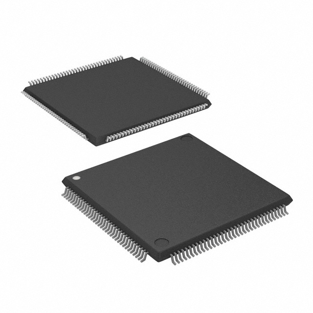
LFXP2-8E-6TN144C
FPGAs

Not available to buy online? Want the lower wholesale price? Please Send RFQ to get best price, we will respond immediately


.png?x-oss-process=image/format,webp/resize,p_30)


LFXP2-8E-6TN144C Description
Lattice Semiconductor's LFXP2-8E-6TN144C is a high-performance field programmable gate array (FPGA) that offers a range of features and applications for various industries.
Description:
The LFXP2-8E-6TN144C is a member of Lattice Semiconductor's low-power, mid-range FPGA family. It is based on the company's advanced 65nm low-power process technology and features a compact 144-ball fine pitch ball grid array (FBGA) package. This FPGA is designed to provide high performance and low power consumption, making it ideal for a wide range of applications.
Features:
- Advanced 65nm low-power process technology: The LFXP2-8E-6TN144C is built using Lattice's 65nm process technology, which enables low power consumption and high performance.
- Compact 144-ball FBGA package: The FPGA is available in a compact 144-ball fine pitch ball grid array package, making it suitable for space-constrained applications.
- High-performance look-up tables (LUTs): The device features a high number of programmable LUTs, which allow for efficient implementation of complex logic functions.
- Dedicated memory resources: The LFXP2-8E-6TN144C includes dedicated memory resources, such as block RAM and register files, to support a wide range of applications.
- Integrated digital signal processing (DSP) blocks: The FPGA includes dedicated DSP blocks, which can be used for high-speed data processing and arithmetic operations.
- High-speed I/O capabilities: The device offers a range of high-speed I/O options, including LVDS, DDR, and gigabit transceivers, to support various interface requirements.
- Configurable power management: The LFXP2-8E-6TN144C features configurable power management, allowing users to optimize power consumption for their specific application.
Applications:
The LFXP2-8E-6TN144C is suitable for a wide range of applications, including but not limited to:
- Industrial control and automation: The FPGA's high performance and low power consumption make it ideal for industrial control systems, motor control, and robotics.
- Communications infrastructure: The high-speed I/O capabilities and DSP blocks make the LFXP2-8E-6TN144C suitable for applications in telecommunications, networking, and data center infrastructure.
- Consumer electronics: The device can be used in various consumer electronics applications, such as set-top boxes, gaming consoles, and smart home devices.
- Automotive: The FPGA's reliability and performance make it suitable for use in automotive applications, such as infotainment systems, advanced driver assistance systems (ADAS), and in-vehicle networking.
- Medical electronics: The LFXP2-8E-6TN144C can be used in medical imaging, patient monitoring, and diagnostic equipment, thanks to its low power consumption and high performance.
- Aerospace and defense: The FPGA's radiation tolerance and high reliability make it suitable for aerospace and defense applications, such as satellite communications, radar systems, and secure communications.
In summary, Lattice Semiconductor's LFXP2-8E-6TN144C is a versatile, high-performance FPGA that offers a range of features and applications for various industries. Its advanced process technology, compact package, and configurable power management make it an ideal choice for demanding applications where performance, power efficiency, and space are critical factors.
Tech Specifications
LFXP2-8E-6TN144C Documents
Download datasheets and manufacturer documentation for LFXP2-8E-6TN144C
Alternate Qualified Test Site 30/Sep/2013 XP2 Family Package Diagrams Product Selector Guide All Dev Pkg Mark Chg 12/Nov/2018 XP2 Family Multiple Devices Cu Wire 01/Jul/2013 Top Mark Format Change 20/Dec/2023 Related Parts


Relevant Search
Shopping Guide


.png?x-oss-process=image/format,webp/resize,h_32)


©2025 ERSA Electronics Corporation.