

Microchip Technology
AT49F040-70PC
Memory ICs Products

Not available to buy online? Want the lower wholesale price? Please Send RFQ to get best price, we will respond immediately


.png?x-oss-process=image/format,webp/resize,p_30)


AT49F040-70PC Description
AT49F040-70PC Description
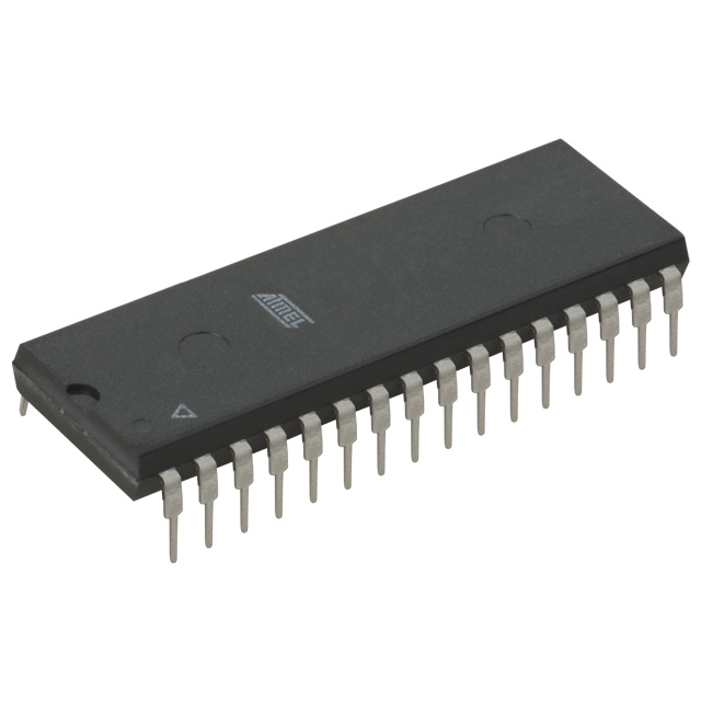
The AT49F040-70PC is a 4Mbit Flash memory IC chip designed by Microchip Technology, featuring a parallel memory interface and packaged in a 32-pin DIP (Dual In-line Package) format. This through-hole mounted device operates within a temperature range of 0°C to 70°C, making it suitable for a variety of industrial and commercial applications. The AT49F040-70PC offers a memory organization of 512K x 8, with an access time of 70 nanoseconds and a write cycle time of 50 microseconds for both word and page operations. It is powered by a supply voltage ranging from 4.5V to 5.5V, ensuring reliable performance across different power supply conditions.
AT49F040-70PC Features
- Memory Organization: The AT49F040-70PC features a 512K x 8 memory organization, providing a total memory size of 4Mbit. This configuration allows for efficient data storage and retrieval, making it ideal for applications requiring substantial memory capacity.
- Access Time: With an access time of 70 nanoseconds, the AT49F040-70PC ensures rapid data access, enhancing the overall performance of systems that require quick memory read operations.
- Write Cycle Time: The device boasts a write cycle time of 50 microseconds for both word and page operations, enabling efficient data writing and minimizing the time required for memory updates.
- Operating Temperature: The AT49F040-70PC operates within a temperature range of 0°C to 70°C, making it suitable for use in environments with moderate temperature variations.
- Voltage Range: The device operates within a supply voltage range of 4.5V to 5.5V, providing flexibility and compatibility with various power supply configurations.
- Parallel Interface: The parallel memory interface of the AT49F040-70PC allows for high-speed data transfer and is compatible with a wide range of systems that utilize parallel memory access.
- Through-Hole Mounting: The through-hole mounting type ensures robust mechanical stability and is well-suited for applications where physical durability is a priority.
- Obsolete Status: While the AT49F040-70PC is marked as obsolete, it remains a viable option for legacy systems and applications where its specific features are still required.
AT49F040-70PC Applications
The AT49F040-70PC is ideal for a range of applications that require reliable and efficient Flash memory solutions. Some specific use cases include:
- Embedded Systems: The device's memory capacity and performance characteristics make it suitable for embedded systems that require non-volatile memory for storing firmware and critical data.
- Industrial Control Systems: The AT49F040-70PC's operating temperature range and robust through-hole mounting make it a reliable choice for industrial control systems that operate in harsh environments.
- Telecommunications: The device's fast access time and write cycle time are beneficial for telecommunications applications where quick data retrieval and updates are essential.
- Consumer Electronics: The AT49F040-70PC can be used in various consumer electronics devices that require non-volatile memory for storing configuration data and software.
- Automotive Systems: The device's operating temperature range and durability make it suitable for automotive applications where reliability and performance are paramount.
Conclusion of AT49F040-70PC
The AT49F040-70PC is a versatile and reliable Flash memory IC chip that offers a balance of performance, capacity, and compatibility. Its 512K x 8 memory organization, fast access and write cycle times, and wide operating temperature range make it suitable for a variety of applications. Despite its obsolete status, the AT49F040-70PC remains a valuable component for systems where its specific features are still required. For designers and engineers seeking a robust and efficient Flash memory solution, the AT49F040-70PC is a compelling choice.
Tech Specifications
AT49F040-70PC Documents
Download datasheets and manufacturer documentation for AT49F040-70PC
AT49F040 Transfer to Microchip/Label/Pkg 5/Sep/2016 AT49F040 Microchip CA Prop65 Microchip RoHS Microchip REACH Related Parts


Shopping Guide


.png?x-oss-process=image/format,webp/resize,h_32)


©2025 ERSA Electronics Corporation.