

Microchip Technology
AT49F512-70JC
Memory ICs Products

Not available to buy online? Want the lower wholesale price? Please Send RFQ to get best price, we will respond immediately


.png?x-oss-process=image/format,webp/resize,p_30)


AT49F512-70JC Description
AT49F512-70JC Description
The AT49F512-70JC is a high-performance Flash memory IC chip manufactured by Microchip Technology. This 512Kbit Flash memory device is organized as 64K x 8 and features a parallel memory interface, making it suitable for a wide range of embedded systems and microcontroller applications. The AT49F512-70JC operates within a voltage range of 4.5V to 5.5V and has an access time of 70 nanoseconds, ensuring fast read operations. The write cycle time for word and page operations is 50 microseconds, providing efficient data storage capabilities.
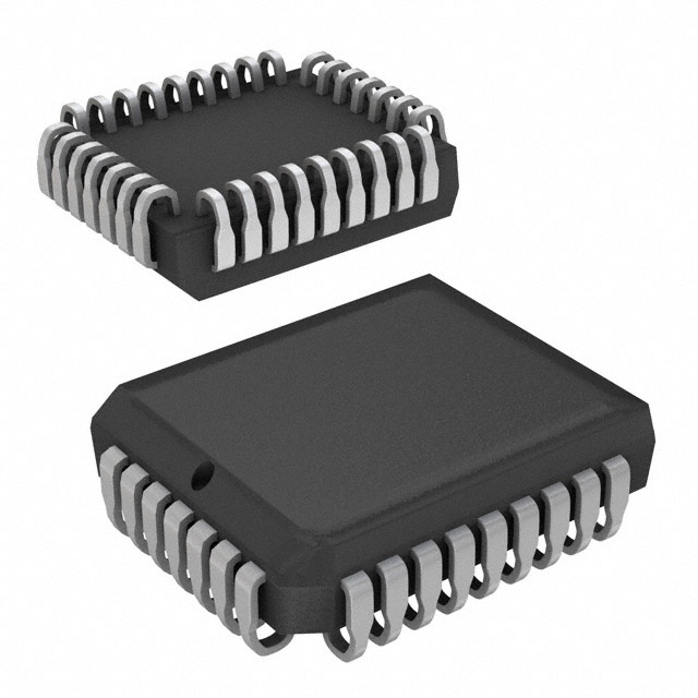
The AT49F512-70JC is housed in a 32-pin PLCC package, which is ideal for surface-mount applications. It is designed to operate within a temperature range of 0°C to 70°C, making it suitable for commercial and industrial environments. The device is categorized under EAR99 for export control and is unaffected by REACH regulations, ensuring compliance with international standards. The moisture sensitivity level (MSL) is rated at 2 (1 Year), indicating its robustness against environmental factors.
AT49F512-70JC Features
- Memory Size and Organization: The AT49F512-70JC offers a total memory size of 512Kbit, organized as 64K x 8, providing ample storage for firmware and data in embedded systems.
- Parallel Interface: The parallel memory interface allows for high-speed data transfer, making it suitable for applications requiring rapid access to stored data.
- Fast Access Time: With an access time of 70 nanoseconds, the AT49F512-70JC ensures quick read operations, enhancing the overall performance of the system.
- Efficient Write Cycle: The write cycle time of 50 microseconds for word and page operations ensures efficient data storage, reducing the time required for firmware updates and data logging.
- Wide Operating Voltage Range: The device operates within a voltage range of 4.5V to 5.5V, providing flexibility in power supply design and ensuring compatibility with various power sources.
- Surface-Mount Packaging: The 32-pin PLCC package is designed for surface-mount technology, facilitating easy integration into compact and high-density PCB designs.
- Commercial Temperature Range: The operating temperature range of 0°C to 70°C makes the AT49F512-70JC suitable for a variety of commercial and industrial applications.
- Compliance and Robustness: The device is categorized under EAR99 for export control and is REACH unaffected, ensuring compliance with international regulations. The MSL rating of 2 (1 Year) ensures robustness against moisture, enhancing reliability in various environments.
AT49F512-70JC Applications
The AT49F512-70JC is ideal for a wide range of applications due to its high-performance characteristics and robust design. Some specific use cases include:
- Embedded Systems: The fast access time and efficient write cycle make it suitable for firmware storage in embedded systems, ensuring quick boot times and reliable operation.
- Microcontroller Applications: The parallel interface and wide operating voltage range make it a perfect companion for microcontrollers, providing non-volatile storage for program code and critical data.
- Industrial Control Systems: The commercial temperature range and surface-mount packaging make it suitable for industrial control systems, where reliability and compact design are crucial.
- Data Logging Devices: The efficient write cycle and ample memory size make it ideal for data logging applications, where frequent data writes are required.
Conclusion of AT49F512-70JC
The AT49F512-70JC is a versatile and high-performance Flash memory IC chip that offers significant advantages over similar models. Its fast access time, efficient write cycle, and robust design make it suitable for a wide range of applications, from embedded systems to industrial control. The device's compliance with international standards and its surface-mount packaging further enhance its appeal for modern electronics design. While the AT49F512-70JC is now considered obsolete, it remains a reliable choice for legacy systems and applications where its unique features and performance benefits are still highly valued.
Tech Specifications
AT49F512-70JC Documents
Download datasheets and manufacturer documentation for AT49F512-70JC
AT49F512 Transfer to Microchip/Label/Pkg 5/Sep/2016 MBB/Label Chgs 16/Nov/2018 AT49F512 Microchip CA Prop65 Microchip RoHS Microchip REACH Related Parts


Shopping Guide


.png?x-oss-process=image/format,webp/resize,h_32)


©2025 ERSA Electronics Corporation.