
 German
 Japanese
 Portuguese
 Korea
Korea
 Mexico
 Dutch
Dutch


Microchip Technology
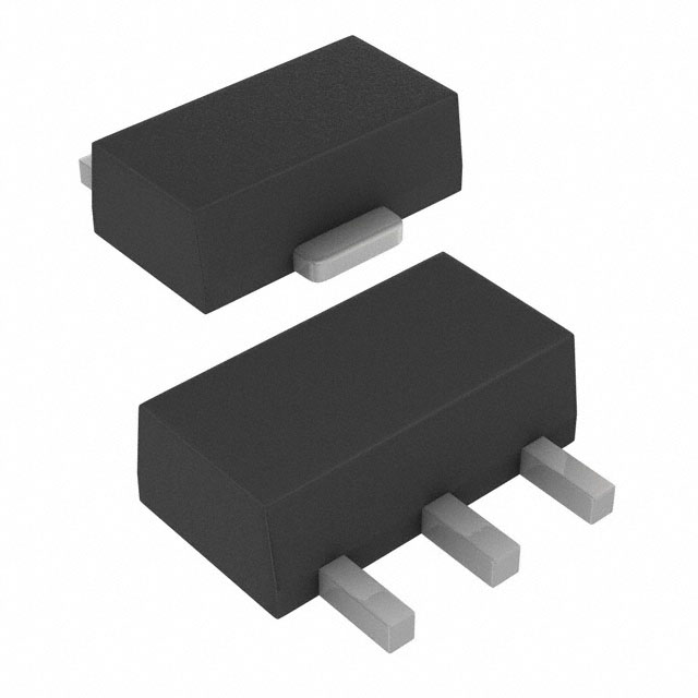
DN3535N8-G

Why Choose Us?
Professional Platform
B2B & B2C purchasingDelivery at full speed
1-2 days deliveryWide variety
Original manufacturers365 days guarantee
Responsible quality
.png)


Tech Specifications
DN3535N8-G Description
DN3535N8-G Description
The DN3535N8-G is a high-performance N-Channel MOSFET from Microchip Technology, designed for applications requiring efficient power management and control. With a drain-to-source voltage (Vdss) of 350V and a continuous drain current (Id) of 230mA at 25°C, it offers robust performance in a variety of electronic systems. This MOSFET features a depletion mode operation, which allows for a wide range of applications, including power switching, motor control, and signal amplification.
DN3535N8-G Features
- Technology: MOSFET (Metal Oxide) - Ensures high efficiency and low power loss.
- Depletion Mode: Offers flexibility in circuit design and operation.
- Input Capacitance (Ciss): 360 pF @ 25 V - Minimizes input capacitance for faster switching.
- Vgs (Max): ±20V - Supports a wide range of gate voltages for compatibility with various control circuits.
- Rds On (Max): 10 Ohm @ 150mA, 0V - Provides low on-resistance for efficient power flow.
- Power Dissipation (Max): 1.6W (Ta) - Capable of handling higher power dissipation for demanding applications.
- Mounting Type: Surface Mount - Ideal for space-constrained designs and high-density PCB layouts.
- Package: Tape & Reel (TR) - Facilitates automated assembly and reduces handling damage.
DN3535N8-G Applications
The DN3535N8-G is well-suited for a variety of applications where high voltage and current handling are required:
- Power Switching: Its high Vdss and low Rds On make it ideal for power management in consumer electronics and industrial control systems.
- Motor Control: The depletion mode operation and high current capability are beneficial for motor drive circuits in robotics and automation.
- Signal Amplification: The low input capacitance and wide Vgs range are advantageous for high-speed signal processing applications.
Conclusion of DN3535N8-G
The DN3535N8-G stands out for its combination of high voltage and current ratings, depletion mode operation, and low on-resistance, making it a versatile choice for demanding electronic applications. Its surface mount package and tape & reel option also cater to modern manufacturing processes. With compliance to RoHS3 and REACH standards, the DN3535N8-G is not only a high-performing component but also an environmentally responsible choice for electronic design engineers.
FAQ
Not available to buy online? Want the lower wholesale price? Please Send RFQ to get best price, we will respond immediately


.png?x-oss-process=image/format,webp/resize,h_32)


