
 German
 Japanese
 Portuguese
 Korea
Korea
 Mexico
 Dutch
Dutch


Microchip Technology
SY89112UMY

Why Choose Us?
Professional Platform
B2B & B2C purchasingDelivery at full speed
1-2 days deliveryWide variety
Original manufacturers365 days guarantee
Responsible quality
.png)


Tech Specifications
SY89112UMY Description
SY89112UMY Description
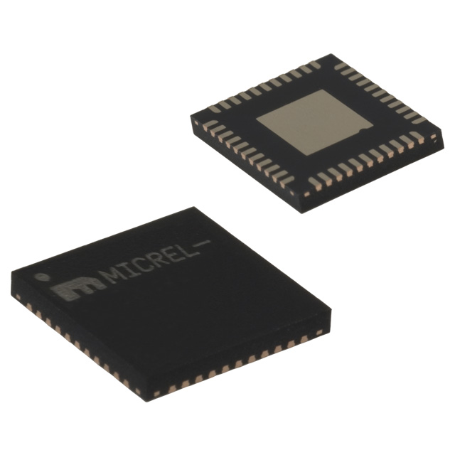
The SY89112UMY is a high-performance clock buffer and multiplexer from Microchip Technology's Precision Edge® series, designed to provide reliable and efficient signal distribution in various electronic systems. This device features a 2:12 input-to-output ratio, supporting a wide range of input and output signal types, including CML, LVDS, and LVPECL. The SY89112UMY operates within a supply voltage range of 2.375V to 3.6V and offers differential signaling on both input and output, ensuring high signal integrity and reduced electromagnetic interference (EMI).
The SY89112UMY is housed in a surface-mount package, making it suitable for compact and space-constrained designs. It has a maximum operating frequency of 3 GHz, providing high-speed signal distribution capabilities. The device is REACH unaffected and RoHS3 compliant, ensuring environmental and regulatory compliance. It is available in a tray package and has a moisture sensitivity level (MSL) of 2 (1 Year), making it suitable for a variety of manufacturing processes.
SY89112UMY Features
- High-Speed Performance: With a maximum operating frequency of 3 GHz, the SY89112UMY is ideal for high-speed signal distribution applications.
- Differential Signaling: Supports differential signaling on both input and output, which helps in reducing EMI and improving signal integrity.
- Versatile Input and Output Types: Compatible with CML, LVDS, and LVPECL input and LVPECL output, offering flexibility in system design.
- Wide Supply Voltage Range: Operates within a supply voltage range of 2.375V to 3.6V, providing compatibility with various power supply configurations.
- Surface-Mount Technology: The surface-mount package allows for easy integration into compact and high-density PCB designs.
- Environmental Compliance: REACH unaffected and RoHS3 compliant, ensuring the device meets stringent environmental and regulatory standards.
- Moisture Sensitivity Level: MSL 2 (1 Year) ensures the device remains stable and reliable during manufacturing and storage processes.
SY89112UMY Applications
The SY89112UMY is well-suited for a variety of applications where high-speed signal distribution and reliability are critical. Some specific use cases include:
- Telecommunications: Ideal for distributing clock signals in high-speed communication systems, ensuring precise timing and synchronization.
- Networking Equipment: Used in routers, switches, and other networking devices to manage clock signals efficiently.
- High-Speed Data Converters: Facilitates the distribution of clock signals in ADCs and DACs, maintaining signal integrity and reducing jitter.
- Test and Measurement Equipment: Provides accurate and reliable clock distribution for precision instruments and test setups.
- Industrial Automation: Ensures robust clock signal distribution in industrial control systems and automation equipment.
Conclusion of SY89112UMY
The SY89112UMY from Microchip Technology is a versatile and high-performance clock buffer and multiplexer that offers significant advantages over similar models. Its wide input and output compatibility, high-speed operation, and differential signaling capabilities make it an ideal choice for a variety of high-speed signal distribution applications. The device's environmental compliance and robust packaging further enhance its reliability and suitability for modern electronic systems. Whether used in telecommunications, networking, or industrial applications, the SY89112UMY provides a reliable and efficient solution for clock signal distribution.
FAQ
| Quantity | Unit Price | Ext. Price |
|---|---|---|
| 1+ | $8.58880 | $8.59 |
| 25+ | $7.15440 | $178.86 |
| 100+ | $6.50320 | $650.32 |
Not available to buy online? Want the lower wholesale price? Please Send RFQ to get best price, we will respond immediately


.png?x-oss-process=image/format,webp/resize,h_32)


