
 German
 Japanese
 Portuguese
 Korea
Korea
 Mexico
 Dutch
Dutch


Microchip Technology
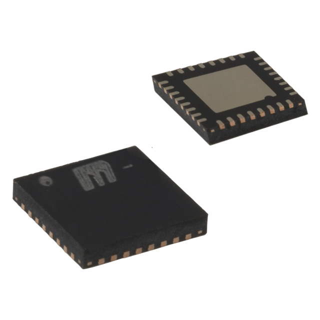
SY89856UMG

Why Choose Us?
Professional Platform
B2B & B2C purchasingDelivery at full speed
1-2 days deliveryWide variety
Original manufacturers365 days guarantee
Responsible quality
.png)


Tech Specifications
SY89856UMG Description
SY89856UMG Description
The SY89856UMG is a high-performance clock buffer and multiplexer from Microchip Technology's Precision Edge® series, designed to provide reliable and efficient signal distribution. This IC features a 2:6 input-to-output ratio, making it ideal for applications requiring fanout buffering and multiplexing of clock signals. The device supports differential signaling, with both input and output stages capable of handling differential signals, ensuring high signal integrity and minimal noise.
The SY89856UMG operates over a supply voltage range of 2.375V to 3.6V, providing flexibility in power supply design. It is designed to work with various input signal types, including CML, LVDS, and PECL, and provides LVPECL outputs, making it versatile for a wide range of applications. The device is housed in a surface-mount package, specifically a 32QFN, which is ideal for compact and high-density PCB layouts.
With a maximum operating frequency of 3 GHz, the SY89856UMG is well-suited for high-speed clock distribution in demanding applications. The device is REACH unaffected and RoHS3 compliant, ensuring it meets the latest environmental and safety standards. The SY89856UMG is available in a tube package, with a moisture sensitivity level (MSL) of 3, allowing for a 168-hour exposure before reflow soldering.
SY89856UMG Features
- High-Speed Performance: Capable of operating up to 3 GHz, ensuring high-speed clock distribution with minimal jitter and skew.
- Differential Signaling: Supports differential inputs and outputs, enhancing signal integrity and reducing electromagnetic interference.
- Versatile Input and Output Types: Compatible with CML, LVDS, and PECL inputs, and provides LVPECL outputs, making it suitable for various signal standards.
- Wide Supply Voltage Range: Operates from 2.375V to 3.6V, offering flexibility in power supply design.
- Surface-Mount Package: The 32QFN package is ideal for compact and high-density PCB layouts, facilitating easy integration into modern electronic systems.
- Environmental Compliance: REACH unaffected and RoHS3 compliant, ensuring adherence to environmental and safety standards.
- Moisture Sensitivity Level: MSL 3 (168 hours), providing flexibility in manufacturing processes without compromising reliability.
SY89856UMG Applications
The SY89856UMG is ideal for a variety of applications in the electronics industry, particularly those requiring high-speed clock distribution and signal integrity. Key applications include:
- Telecommunications: High-speed clock distribution in base stations, switches, and routers.
- Data Centers: Efficient signal distribution in servers and storage systems.
- High-Speed Computing: Clock buffering in high-performance computing systems and GPUs.
- Industrial Automation: Reliable clock distribution in industrial control systems and PLCs.
- Consumer Electronics: Signal distribution in high-speed interfaces such as HDMI and DisplayPort.
Conclusion of SY89856UMG
The SY89856UMG from Microchip Technology is a robust and versatile clock buffer and multiplexer, offering high-speed performance, differential signaling, and compatibility with various input and output types. Its wide supply voltage range, surface-mount package, and environmental compliance make it an excellent choice for a wide range of applications. Whether used in telecommunications, data centers, or high-speed computing, the SY89856UMG ensures reliable signal distribution and high performance, making it a standout solution in the electronics industry.
FAQ
| Quantity | Unit Price | Ext. Price |
|---|---|---|
| 1+ | $8.22800 | $8.23 |
| 25+ | $6.87280 | $171.82 |
| 100+ | $6.24800 | $624.80 |
Not available to buy online? Want the lower wholesale price? Please Send RFQ to get best price, we will respond immediately


.png?x-oss-process=image/format,webp/resize,h_32)


