Micron Technology_MT29F4G08ABBEAH4:E
original

Micron Technology
MT29F4G08ABBEAH4:E

774-MT29F4G08ABBEAH4:E
PDF Datasheet
IC FLASH 4GBIT PARALLEL 63VFBGA

Why Choose Us?

Professional Platform

B2B & B2C purchasing

Delivery at full speed

1-2 days delivery

Wide variety

Original manufacturers

365 days guarantee

Responsible quality
APAC
ISO9001
Quality Policy
ISO45001
ISO14001
Original

Tech Specifications

Operating Temperature
0°C ~ 70°C (TA)
Memory Interface
Parallel
ECCN
3A991B1A
Memory Organization
512M x 8
Mounting Type
Surface Mount
Memory Type
Non-Volatile
Product Status
Obsolete
Supplier Device Package
63-VFBGA (9x11)
Show More

MT29F4G08ABBEAH4:E Description

Micron Technology, Inc.

MT29F4G08ABBEAH4:E

4Gb (512M x 8) SLC NAND Flash Memory · 3.3V Supply · Asynchronous Parallel Interface · 48-pin TSOP
🧠 4Gb Density (512MB) ⚡ 2.7V – 3.6V Supply ⏱️ 25ns Access Time 📦 48-pin TSOP (12×20mm) 🌡️ 0°C to +70°C (Commercial)

📖 Product Overview

The MT29F4G08ABBEAH4:E is a 4,294,967,296‑bit (4Gb) Single‑Level Cell (SLC) NAND Flash memory from Micron Technology, organized as 536,870,912 words × 8 bits (512M x 8). It provides high‑density, reliable non‑volatile storage for embedded systems, solid‑state drives, and consumer electronics that require cost‑effective mass storage with simple asynchronous parallel interface.

The device operates from a single 3.3V power supply (2.7V – 3.6V) and features a fast 25ns random access time (tRC). The NAND Flash architecture is organized with 2KB page size (2,112 bytes including spare) and 64‑page erase blocks (128KB + spare per block). It supports standard NAND Flash commands and uses an asynchronous parallel interface with multiplexed address/data lines (I/O[7:0]). The device includes a Ready/Busy (R/B) output for program/erase status monitoring.

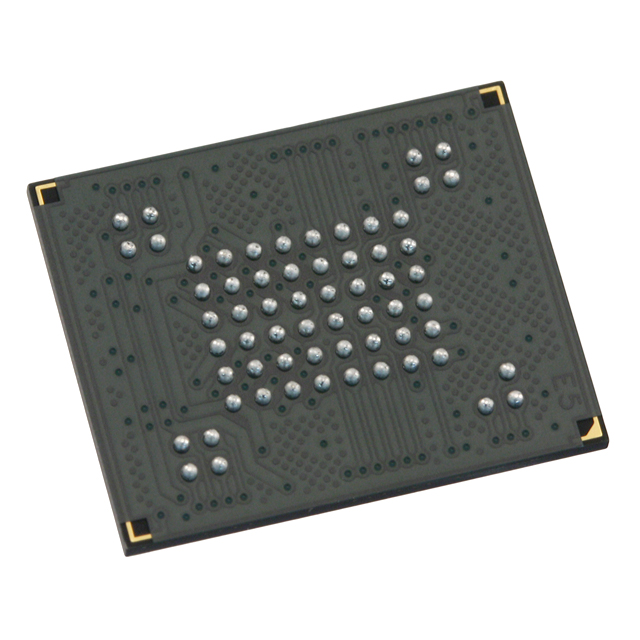
The MT29F4G08ABBEAH4:E is housed in a 48‑pin TSOP Type I package (12mm × 20mm × 1.2mm), which is widely used for NAND Flash components in PCB designs. It is supplied in trays and is fully RoHS compliant (lead‑free). The device supports a minimum of 100,000 program/erase cycles and guarantees 10 years data retention. The ":E" suffix indicates a specific configuration (likely a particular die revision or packaging variant).

📋 Technical Specifications

Density
4 Gbit (4,294,967,296 bits) / 512 MB
Organization
512M x 8 (536,870,912 words × 8 bits)
Memory Type
SLC NAND Flash
Interface
Asynchronous parallel (multiplexed address/data)
Access Time (tRC)
25ns (max)
Page Size (Main + Spare)
2,112 bytes (2,048 + 64)
Block Size
135,168 bytes (64 pages)
Number of Blocks
2,048 (total memory array)
Supply Voltage (Vcc)
2.7V – 3.6V
Active Current (Read)
20 mA (typical)
Standby Current
30 µA (typical)
Page Program Time (Typ)
200 μs
Block Erase Time (Typ)
2 ms
Programming/Erase Cycles
100,000 (minimum)
Data Retention
10 years (minimum)
Operating Temperature
0°C to +70°C (Commercial)

✨ Key Features

SLC NAND Technology – High reliability and endurance
Asynchronous Parallel Interface – Simple legacy NAND controller interface
Fast Access Time – 25ns tRC for random read
Efficient Page Program – 200μs typical page programming
Fast Block Erase – 2ms typical block erase time
Ready/Busy (R/B) Output – Easy program/erase status monitoring
Hardware Write Protect – Protects the first block (WP pin)
Copy Back Feature – Fast internal data copy without external bus cycles
High Endurance – 100,000 program/erase cycles
Long Data Retention – 10 years minimum
Standard 48-pin TSOP Package – 12mm × 20mm, 0.5mm lead pitch
RoHS Compliant & Lead‑Free – Environmentally friendly packaging

🎯 Typical Applications

Embedded Systems & Boot Code Storage Solid‑State Drives (SSD) and USB Flash Drives Digital Cameras & Portable Media Players Set‑Top Boxes & Digital TVs Printers & Multifunction Peripherals Telecom & Networking Equipment (legacy designs) Medical Devices & Diagnostic Instruments Legacy System Maintenance & Upgrades
Page Program Time
200 μs
Typical page program time
Block Erase Time
2 ms
Typical erase time (64‑page block)
Package Type
TSOP-48
12mm × 20mm, 0.5mm lead pitch
🔍 Part Number Decoding (MT29F4G08ABBEAH4:E)
MT29F – Micron NAND Flash family
4G08 – 4Gb density, x8 organisation
A – Voltage: 3.3V
BB – Die technology / block size (2KB page, 64 pages/block)
EA – Package & design revision (48-pin TSOP, 12×20mm)
H4 – Commercial temperature (0°C to +70°C)
:E – Specific configuration / firmware version
⚠️ The MT29F4G08ABBEAH4:E is considered obsolete (not recommended for new designs). For legacy system maintenance and existing designs only. Contact Micron for replacement or upgrade options.
Information compiled from Micron NAND Flash product documentation (legacy datasheets) and industry standards.

FAQ

What is the MT29F4G08ABBEAH4:E?
A: The MT29F4G08ABBEAH4:E is a 4‑gigabit (4Gb) SLC NAND Flash memory device manufactured by Micron Technology. It is organized as 512M × 8 bits (512 million words × 8 bits), providing a total memory capacity of 512 megabytes (512 MB). The device uses a parallel asynchronous interface and is fully compliant with the Open NAND Flash Interface (ONFI) 1.0 specification [12†L10-L11]. It is housed in a 63‑ball VFBGA (9 × 11 mm) package and is designed for high‑reliability code and data storage in embedded, industrial, and consumer applications [5†L14-L15][6†L3]. The "E" in the part number indicates the design revision level, and the commercial temperature grade (0°C to +70°C) version is identified by the suffix "H4:E" (vs. the industrial "H4-IT:E" variant) [7†L8-L10][11†L5-L9].
What are the key technical features and specifications?
What interface does the MT29F4G08ABBEAH4:E use and how does it communicate with a host processor?
What are the endurance, data retention, and reliability specifications?
What applications is the MT29F4G08ABBEAH4:E intended for, and what is its current lifecycle status?
Quick Quote
ADD TO RFQ LIST

Not available to buy online? Want the lower wholesale price? Please Send RFQ to get best price, we will respond immediately

QUICK RFQ