
 German
 Japanese
 Portuguese
 Korea
Korea
 Mexico
 Dutch
Dutch


Micron Technology
MT47H64M16NF-25E IT:M

Why Choose Us?
Professional Platform
B2B & B2C purchasingDelivery at full speed
1-2 days deliveryWide variety
Original manufacturers365 days guarantee
Responsible quality
.png)


Tech Specifications
MT47H64M16NF-25E IT:M Description
MT47H64M16NF-25E IT:M
1Gb (64M x16) Industrial DDR2 SDRAM | 1.8V | 400MHz | -40°C to +95°C | 84-ball FBGA
Micron
Density
Clock Frequency
Data Rate
VDD / VDDQ
8x12.5mm
Product Overview
The Renesas Electronics Corporation (formerly Micron Technology) MT47H64M16NF-25E IT:M is a 1Gb (1,073,741,824 bits) DDR2 SDRAM component organized as 64M words × 16 bits. Operating at a low 1.8V nominal voltage (±0.1V), it achieves a clock frequency of 400 MHz (800 Mbps data rate per pin) with a CAS latency of CL = 5.[reference:0] The “-25E” timing parameter indicates a 2.5 ns cycle time (tCK), standard for DDR2‑800 operation. This device is designed for high‑performance embedded, industrial, networking, and telecommunication applications requiring reliable memory in harsh environments.
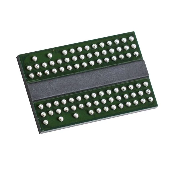
The IT:M suffix denotes the industrial temperature grade, with an extended operating temperature range of -40°C to +95°C, making it suitable for outdoor and industrial control systems.[reference:1] Housed in a standard 84‑ball Thin Fine-Pitch Ball Grid Array (TFBGA) package measuring 8.00mm × 12.50mm × 1.20mm, the MT47H64M16NF-25E IT:M delivers the performance, power efficiency, and long‑term reliability required for advanced embedded computing platforms.[reference:2]
📊 Technical Specifications
| Density / Organization | 1Gb (64M × 16 bits) |
| Memory Interface | Parallel (JEDEC DDR2 SDRAM command/address bus, 16‑bit DQ) |
| Clock Frequency (Max) | 400 MHz — DDR2‑800 speed grade [reference:3] |
| Data Rate | 800 Mbps per pin [reference:4] |
| Peak Bandwidth | 1.6 GB/s (x16 @ 800 Mbps) |
| Supply Voltage (VDD / VDDQ) | 1.7V – 1.9V (1.8V nominal) [reference:5] |
| Operating Temperature | Industrial: -40°C to +95°C [reference:6] |
| Storage Temperature | -55°C to +100°C |
| Package Type | 84‑ball TFBGA (8.00mm × 12.50mm × 1.20mm, 0.8mm pitch) — NF package code [reference:7] |
| Package Dimensions | 8.00 × 12.50 × 1.20 mm [reference:8] |
| CAS Latency (CL) | CL = 5 @ 400MHz [reference:9] |
| Number of Banks | 8 internal banks for concurrent operation [reference:10] |
| Refresh | 64ms, 8192 cycles (8K AREF), AUTO and SELF REFRESH [reference:11] |
| Low Power Features | Posted CAS additive latency (AL), power‑down modes, temperature‑compensated refresh |
| On‑Die Termination (ODT) | Programmable RTT values improve signal integrity [reference:12] |
| Prefetch Architecture | 4n‑bit prefetch [reference:13] |
| Burst Length | 4 or 8 (programmable) [reference:14] |
| I/O Standard | SSTL_18 (1.8V I/O), JEDEC standard[reference:15] |
| Differential Strobe | DQS, DQS# for precise data capture |
| Access Time (tAC) | 400 ps (maximum) [reference:16] |
| RoHS / Halogen Free | Yes — “:M” suffix indicates green, lead‑free |
| Moisture Sensitivity Level | MSL 3 |
| Part Status | Active — In production [reference:17] |
✨ Key Features
- ✅ Extended Industrial Temperature Range – -40°C to +95°C (Tc), ideal for outdoor, telecom, and industrial applications
- ✅ 1.8V Low‑Power Operation – VDD = VDDQ = 1.7V–1.9V, reduces power consumption while maintaining high performance
- ✅ High‑Speed 400MHz / 800Mbps – 1.6 GB/s bandwidth per component, supporting high‑throughput embedded processing
- ✅ 8 Internal Banks – Enables concurrent operations and reduces row cycle conflicts
- ✅ Programmable CAS Latency – CL = 5/4/3 for flexible timing adaptation
- ✅ Posted CAS Additive Latency (AL) – Improves bus efficiency by hiding command overhead
- ✅ Selectable Burst Length (BL) – Supports BL = 4 or 8 to match application needs
- ✅ On‑Die Termination (ODT) – Programmable 50Ω/75Ω/150Ω termination for better signal integrity
- ✅ Differential Data Strobe (DQS, DQS#) – Enables robust data capture at 800 Mbps
- ✅ DLL (Delay‑Locked Loop) – Aligns DQ and DQS transitions with clock edges for precise timing
- ✅ Auto and Self Refresh – Supports 64ms refresh (8K cycle) with temperature‑compensated options
- ✅ Adjustable Data‑Output Drive Strength – Optimizes signal amplitude for system‑specific loading
- ✅ JEDEC Standard 1.8V I/O (SSTL_18‑compatible) – Drop‑in compatible with industry‑standard DDR2 controllers
- ✅ 4n‑bit Prefetch Architecture – Delivers high internal read/write bandwidth with lower clock rates
- ✅ Industrial Quality & Long‑term Availability – Backed by Micron’s and Renesas’ commitment to extended product lifecycles
⚡ DDR2 SDRAM Architecture & Performance
The MT47H64M16NF-25E IT:M is optimized for systems requiring high memory bandwidth in extended temperature environments. Its 1.8V operation, 8‑bank architecture, and programmable timing parameters make it a versatile choice for industrial and embedded computing applications where reliability and longevity are critical.
🔒 Advanced DDR2 Features
🔧 Programmable READ and WRITE Latencies
The device supports independent READ latency (CAS Latency + Additive Latency) and WRITE latency (READ latency – 1), allowing the memory controller to optimize command scheduling for maximum bus utilization.
📊 Data Strobe (DQS) with Differential Options
Differential data strobes (DQS, DQS#) provide precise capture windows for read and write operations, reducing system timing margin requirements.
🛡️ Temperature‑Compensated Self‑Refresh
The device automatically adjusts self‑refresh rate based on temperature, reducing power consumption at lower temperatures while maintaining data integrity at higher temperatures.
⏰ DLL (Delay‑Locked Loop)
An internal DLL aligns DQ and DQS transitions with the system clock (CK), compensating for process, voltage, and temperature (PVT) variations.
📦 Ordering Information & Part Number Decoder
| Orderable Part Number | Speed / Temp | Package | Description |
|---|---|---|---|
| MT47H64M16NF-25E IT:M | DDR2‑800 / -40°C to +95°C | 84‑TFBGA | Industrial temperature, tray (1368 pcs/tray) |
| MT47H64M16NF-25E IT:M TR | DDR2‑800 / -40°C to +95°C | 84‑TFBGA | Industrial, tape & reel (2000 pcs/reel) [reference:18] |
| MT47H64M16NF-25E AIT:M | DDR2‑800 / -40°C to +95°C | 84‑TFBGA | Automotive Grade 2 (AEC‑Q100) [reference:19] |
| MT47H64M16NF-25E IT:M (Tube) | DDR2‑800 / -40°C to +95°C | 84‑TFBGA | Tray packaging (standard) |
• MT47H – Micron DDR2 SDRAM family
• 64M16 – 64M × 16 = 1Gb density
• NF – 84‑ball TFBGA package (8×12.5mm, 0.8mm pitch)
• 25E – Speed bin: 2.5ns cycle time (DDR2‑800, CL=5)
• IT – Industrial temperature range (-40°C to +95°C)
• :M – Green, lead‑free, halogen‑free, RoHS compliant
🏆 Renesas Electronics – Global Leader in Embedded Memory
Renesas Electronics Corporation (following its acquisition of Micron’s industrial DRAM portfolio) is a world‑leading semiconductor supplier, offering a comprehensive portfolio of microcontrollers, memory, analog, and power solutions. The MT47H family of DDR2 SDRAM components is designed for industrial and embedded applications requiring long lifecycles, extended temperature support, and proven reliability.
- #1 Global MCU supplier – trusted by leading industrial and automotive OEMs worldwide
- AEC‑Q100 qualified automotive grade options for DDR2 and DDR3L components
- ISO 9001, ISO 14001, IATF 16949 certified manufacturing facilities
- 15‑20 year product lifecycle support – long‑term availability for industrial designs
- Global FAE support – free samples, evaluation platforms, and reference designs
🛠️ Development Resources & Support
Renesas offers free samples, evaluation platforms, and direct FAE support through authorized distributors. For automotive PPAP documentation, industrial reliability reports, and design‑in assistance, contact your local Renesas sales office.
📄 Certifications & Compliance
- RoHS 2011/65/EU (Compliant)
- REACH SVHC (Compliant)
- Halogen‑free per IEC 61249-2-21
- Conflict Minerals (CFSI) report available
- JEDEC JESD79‑2F compliant
📦 Packaging & Logistics
- Tray: 1368 pieces per tray (TFBGA)
- Tape & Reel: 2000 pieces per 13" reel
- Moisture Sensitivity Level: MSL 3
- Lead finish: SnAgCu (SAC305) – green, lead‑free
- Lead time: 8‑10 weeks ARO, stock available via distributors
FAQ
| Quantity | Unit Price | Ext. Price |
|---|---|---|
| 1+ | $4.59085 | $4.59 |
| 10+ | $3.90685 | $39.07 |
| 30+ | $3.49885 | $104.97 |
| 100+ | $2.96057 | $296.06 |
| 500+ | $2.77028 | $1385.14 |
Not available to buy online? Want the lower wholesale price? Please Send RFQ to get best price, we will respond immediately


.png?x-oss-process=image/format,webp/resize,h_32)


