
 German
 Japanese
 Portuguese
 Korea
Korea
 Mexico
 Dutch
Dutch


Microsemi
M2S010S-1FGG484I

Why Choose Us?
Professional Platform
B2B & B2C purchasingDelivery at full speed
1-2 days deliveryWide variety
Original manufacturers365 days guarantee
Responsible quality
.png)


Tech Specifications
M2S010S-1FGG484I Description
M2S010S-1FGG484I Description
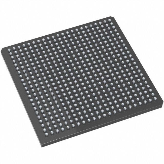
The M2S010S-1FGG484I is an advanced System-on-Chip (SoC) from Microsemi Corporation, part of the SmartFusion®2 series. This embedded IC chip is designed to offer a blend of high performance and flexibility, making it suitable for a wide range of applications. The M2S010S-1FGG484I features a 166MHz ARM Cortex-M3 processor, combining the capabilities of a microcontroller (MCU) and a field-programmable gate array (FPGA). It is housed in a 484-pin BGA package, ensuring robustness and reliability in various operating conditions.
M2S010S-1FGG484I Features
- High-Speed Performance: The M2S010S-1FGG484I operates at a speed of 166MHz, providing rapid processing capabilities essential for demanding applications.
- Dual Architecture: The integration of MCU and FPGA functionalities allows for both high-level programming and low-level hardware customization, offering unparalleled flexibility.
- Memory Capacity: With 256KB of flash memory and 64KB of RAM, the M2S010S-1FGG484I can handle complex tasks and store significant amounts of data.
- Enhanced Connectivity: The chip supports a variety of connectivity options, including CANbus, Ethernet, I2C, SPI, UART/USART, and USB, making it ideal for networked and IoT applications.
- Peripheral Integration: The inclusion of DDR, PCIe, and SERDES peripherals enhances the chip's ability to manage high-speed data transfers and complex communication protocols.
- I/O Capabilities: The M2S010S-1FGG484I boasts 233 I/O pins, providing extensive connectivity options for interfacing with various external devices.
- Regulatory Compliance: The chip is classified under ECCN 5A002A1 and HTSUS 8542.39.0001, ensuring compliance with international export regulations. It is also REACH unaffected, meeting environmental and safety standards.
- Packaging and Sensitivity: The M2S010S-1FGG484I is packaged in a tray format with a moisture sensitivity level (MSL) of 3, allowing for 168 hours of exposure before reflow soldering.
M2S010S-1FGG484I Applications
The M2S010S-1FGG484I is designed for applications requiring high performance, flexibility, and robust connectivity. Its unique features make it ideal for:
- Industrial Automation: The combination of high-speed processing and extensive I/O capabilities allows for efficient control and monitoring of industrial processes.
- Telecommunications: The chip's advanced connectivity options, including Ethernet and PCIe, make it suitable for networking equipment and communication infrastructure.
- Automotive Systems: The M2S010S-1FGG484I can be used in advanced driver assistance systems (ADAS) and vehicle control units, leveraging its high-speed processing and reliable performance.
- Medical Devices: The chip's flexibility and robustness make it suitable for medical equipment requiring precise control and data processing.
- Aerospace and Defense: The M2S010S-1FGG484I's high performance and compliance with stringent regulatory standards make it ideal for applications in aerospace and defense sectors.
Conclusion of M2S010S-1FGG484I
The M2S010S-1FGG484I from Microsemi Corporation is a versatile and powerful SoC that combines the strengths of an ARM Cortex-M3 processor with FPGA capabilities. Its high-speed performance, extensive memory, and robust connectivity options make it suitable for a wide range of applications, from industrial automation to aerospace and defense. Despite being marked as obsolete, the M2S010S-1FGG484I remains a valuable component for engineers and designers seeking a reliable and flexible solution for their projects.
FAQ
Not available to buy online? Want the lower wholesale price? Please Send RFQ to get best price, we will respond immediately


.png?x-oss-process=image/format,webp/resize,h_32)


