
 German
 Japanese
 Portuguese
 Korea
Korea
 Mexico
 Dutch
Dutch


Microsemi
M2S100S-1FC1152I

Why Choose Us?
Professional Platform
B2B & B2C purchasingDelivery at full speed
1-2 days deliveryWide variety
Original manufacturers365 days guarantee
Responsible quality
.png)


Tech Specifications
M2S100S-1FC1152I Description
M2S100S-1FC1152I Description
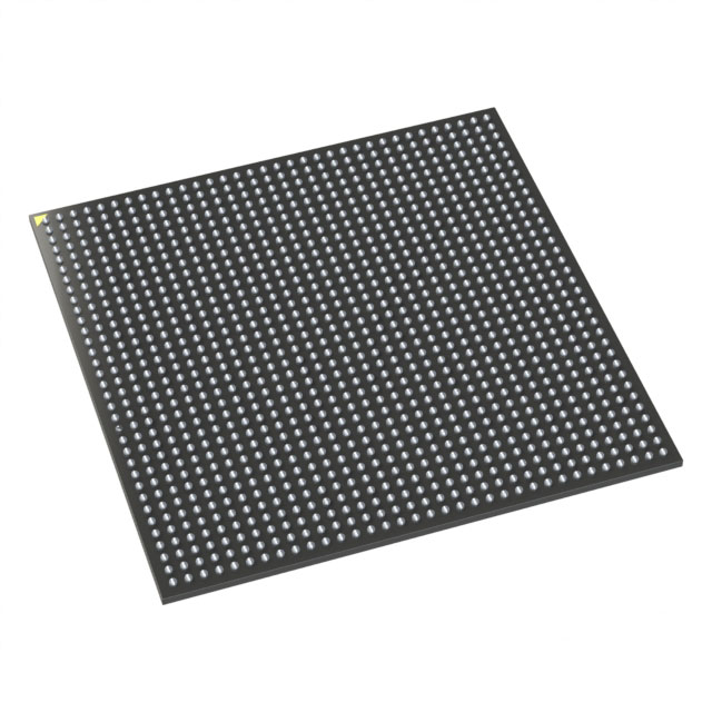
The M2S100S-1FC1152I is an advanced System on Chip (SoC) from Microsemi Corporation, part of the SmartFusion®2 series. This embedded IC chip integrates a Cortex-M3 microcontroller (MCU) and Field Programmable Gate Array (FPGA) architecture, offering a powerful combination of processing capabilities and programmable logic. The M2S100S-1FC1152I operates at a clock speed of 166MHz, providing high-performance processing for demanding applications. It features 512KB of flash memory and 64KB of RAM, ensuring ample storage and fast data access. The chip is housed in a 1152-ball BGA package, making it suitable for compact and high-density designs. With 574 I/O pins and a range of peripherals including DDR, PCIe, and SERDES, the M2S100S-1FC1152I offers extensive connectivity options. The chip also supports multiple communication protocols such as CANbus, Ethernet, I2C, SPI, UART/USART, and USB, enhancing its versatility in various embedded systems.
M2S100S-1FC1152I Features
- High-Speed Performance: The M2S100S-1FC1152I operates at 166MHz, providing efficient and fast processing capabilities essential for real-time applications.
- Integrated MCU and FPGA: Combines a Cortex-M3 microcontroller with FPGA programmable logic, offering a flexible and powerful solution for complex system designs.
- Robust Memory: Equipped with 512KB of flash memory and 64KB of RAM, ensuring sufficient storage for firmware and data handling.
- Extensive I/O and Peripherals: Features 574 I/O pins and supports DDR, PCIe, and SERDES, making it ideal for applications requiring high-speed data transfer and interfacing.
- Multiple Connectivity Options: Supports CANbus, Ethernet, I2C, SPI, UART/USART, and USB, facilitating seamless integration into various communication networks.
- Compliance and Safety: Classified under ECCN 3A001A7A and HTSUS 8542.39.0001, and is REACH unaffected, ensuring compliance with international regulations.
- Packaging and Sensitivity: Available in a tray package with a moisture sensitivity level (MSL) of 3 (168 hours), suitable for standard manufacturing processes.
M2S100S-1FC1152I Applications
The M2S100S-1FC1152I is ideal for a wide range of applications due to its versatile architecture and extensive feature set. Some specific use cases include:
- Industrial Automation: The combination of high-speed processing and extensive I/O capabilities make it suitable for controlling and monitoring complex industrial processes.
- Telecommunications: The support for multiple communication protocols and high-speed interfaces enables its use in networking equipment and communication infrastructure.
- Medical Devices: The robust memory and processing power allow for the development of advanced medical devices requiring real-time data processing and storage.
- Automotive Systems: The chip’s ability to handle multiple communication protocols and its high-speed performance make it ideal for automotive applications such as engine control units and advanced driver-assistance systems (ADAS).
- Consumer Electronics: The M2S100S-1FC1152I can be used in high-end consumer electronics where compact design and high performance are critical.
Conclusion of M2S100S-1FC1152I
The M2S100S-1FC1152I from Microsemi Corporation is a versatile and powerful SoC that offers a unique blend of high-speed processing, extensive memory, and flexible programmable logic. Its integration of Cortex-M3 MCU and FPGA architecture, combined with a wide range of I/O options and communication protocols, makes it a standout choice for various embedded applications. Despite being marked as obsolete, the M2S100S-1FC1152I remains a reliable and capable solution for developers seeking a robust and feature-rich embedded IC chip.
FAQ
Not available to buy online? Want the lower wholesale price? Please Send RFQ to get best price, we will respond immediately


.png?x-oss-process=image/format,webp/resize,h_32)


