
 German
 Japanese
 Portuguese
 Korea
Korea
 Mexico
 Dutch
Dutch


Nexperia
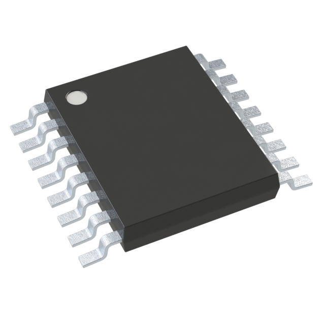
74HC4051PW,112

Why Choose Us?
Professional Platform
B2B & B2C purchasingDelivery at full speed
1-2 days deliveryWide variety
Original manufacturers365 days guarantee
Responsible quality
.png)


Tech Specifications
74HC4051PW,112 Description
74HC4051PW,112 Description
The 74HC4051PW,112 is an 8-channel analog multiplexer/demultiplexer from Nexperia, designed for high-performance signal routing in mixed-signal applications. Housed in a 16-pin TSSOP package, this IC features low on-state resistance (120Ω max) and minimal channel-to-channel matching (ΔRon = 6Ω), ensuring consistent signal integrity. It supports dual-supply voltage (±1.5V to ±5V) or single-supply (2V to 10V), making it versatile for both low-voltage and standard logic applications. With a -3dB bandwidth of 180MHz and fast switching times (Ton = 51ns, Toff = 42ns), it excels in high-speed signal switching.
74HC4051PW,112 Features
- Low Leakage Current: Max 400nA ensures minimal power loss in off-state.
- High Bandwidth: 180MHz enables use in RF and high-frequency analog systems.
- Low Capacitance: 3.5pF channel capacitance reduces signal distortion.
- Wide Voltage Range: Compatible with ±5V dual-supply or 10V single-supply configurations.
- Robust Performance: ROHS3 compliant and REACH unaffected, meeting environmental standards.
- Surface-Mount Design: TSSOP-16 package optimizes PCB space in compact designs.
74HC4051PW,112 Applications
- Test & Measurement Equipment: Precision signal routing in oscilloscopes or data acquisition systems.
- Audio/Video Switching: Low-distortion multiplexing in AV receivers or broadcast systems.
- Battery-Powered Devices: Efficient signal selection in portable electronics due to low leakage.
- Industrial Control Systems: Reliable multiplexing for sensor arrays or PLCs.
- Telecommunications: High-frequency signal routing in RF modules or base stations.
Conclusion of 74HC4051PW,112
The 74HC4051PW,112 stands out for its low on-resistance, high bandwidth, and dual-supply flexibility, making it ideal for mixed-signal and high-speed applications. While marked as obsolete, its performance remains competitive for legacy designs or replacements. Engineers value its low distortion, fast switching, and compact form factor, particularly in test equipment, audio systems, and industrial controls. For projects requiring reliable analog multiplexing with minimal signal degradation, this IC remains a strong candidate.
FAQ
| Quantity | Unit Price | Ext. Price |
|---|---|---|
| 833+ | $0.31680 | $263.89 |
Not available to buy online? Want the lower wholesale price? Please Send RFQ to get best price, we will respond immediately


.png?x-oss-process=image/format,webp/resize,h_32)


