
 German
 Japanese
 Portuguese
 Korea
Korea
 Mexico
 Dutch
Dutch


Nexperia
74HC4052D-Q100,118

Why Choose Us?
Professional Platform
B2B & B2C purchasingDelivery at full speed
1-2 days deliveryWide variety
Original manufacturers365 days guarantee
Responsible quality
.png)


Tech Specifications
74HC4052D-Q100,118 Description
74HC4052D-Q100,118 Description
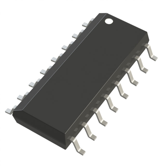
The 74HC4052D-Q100,118 is a high-performance, automotive-grade interface IC chip designed for demanding applications requiring reliable and efficient signal routing. Manufactured by Nexperia USA Inc., this device features a 4:1 multiplexer/demultiplexer circuit with dual SP4T (Single Pole, Four Throw) switch circuits, providing versatile signal switching capabilities. The 74HC4052D-Q100,118 is housed in a surface-mount 16SO package, making it suitable for compact and high-density PCB designs.
74HC4052D-Q100,118 Features
- Low Leakage Current: With a maximum leakage current (IS(off)) of 2µA, the 74HC4052D-Q100,118 ensures minimal power consumption and signal degradation, making it ideal for low-power applications.
- Wide Supply Voltage Range: The device operates with a dual supply voltage range of ±1.5V to ±5V and a single supply voltage range of 2V to 10V, providing flexibility in various power supply configurations.
- High Channel Matching: The channel-to-channel matching (ΔRon) is 6Ω, ensuring consistent performance across multiple channels.
- Low Channel Capacitance: With a channel capacitance (CS(off), CD(off)) of 3.5pF, the 74HC4052D-Q100,118 minimizes signal distortion and crosstalk.
- Low On-State Resistance: The maximum on-state resistance (Ron) is 150Ω, facilitating efficient signal transmission with minimal power loss.
- Fast Switching Time: The switch time (Ton, Toff) is 58ns and 48ns respectively, enabling rapid signal switching and high-speed operation.
- High Bandwidth: The -3dB bandwidth is 180MHz, supporting high-frequency signal routing.
- Automotive Grade: Certified for automotive applications, the 74HC4052D-Q100,118 meets stringent reliability and performance standards.
- Compliance: The device is REACH unaffected and RoHS3 compliant, ensuring environmental safety and regulatory adherence.
- Moisture Sensitivity Level: With an MSL of 1 (Unlimited), the 74HC4052D-Q100,118 is suitable for various manufacturing environments without moisture-related concerns.
74HC4052D-Q100,118 Applications
The 74HC4052D-Q100,118 is well-suited for a variety of applications, particularly in the automotive sector, where reliability and performance are paramount. Key applications include:
- Automotive Electronics: Ideal for in-vehicle infotainment systems, advanced driver-assistance systems (ADAS), and other automotive electronic modules requiring robust signal switching.
- Signal Routing: Efficiently routes analog and digital signals in complex electronic systems, ensuring high signal integrity and minimal interference.
- High-Speed Data Transmission: Suitable for applications requiring high-speed data transmission, such as communication interfaces and sensor networks.
- Industrial Control Systems: Provides reliable signal switching in industrial automation and control systems, enhancing system performance and reliability.
Conclusion of 74HC4052D-Q100,118
The 74HC4052D-Q100,118 is a versatile and high-performance interface IC chip designed to meet the stringent demands of automotive and industrial applications. Its low leakage current, wide supply voltage range, and fast switching time make it an excellent choice for applications requiring efficient signal routing and minimal power loss. The device's automotive-grade certification and compliance with environmental regulations further enhance its suitability for modern electronic systems. Whether used in automotive electronics, signal routing, or high-speed data transmission, the 74HC4052D-Q100,118 offers reliable and efficient performance, making it a standout choice in its category.
FAQ
| Quantity | Unit Price | Ext. Price |
|---|---|---|
| 1+ | $0.43120 | $0.43 |
| 10+ | $0.29744 | $2.97 |
| 50+ | $0.24517 | $12.26 |
| 100+ | $0.22889 | $22.89 |
| 2500+ | $0.18396 | $459.90 |
Not available to buy online? Want the lower wholesale price? Please Send RFQ to get best price, we will respond immediately


.png?x-oss-process=image/format,webp/resize,h_32)


