
Nexperia
74HCT367D,652

Why Choose Us?
Professional Platform
B2B & B2C purchasingDelivery at full speed
1-2 days deliveryWide variety
Original manufacturers365 days guarantee
Responsible quality
.png)


Tech Specifications
74HCT367D,652 Description
74HCT367D,652 Description
The 74HCT367D,652 is a non-inverting buffer IC designed for high-speed data transmission and signal conditioning. Manufactured by Nexperia USA Inc., this device belongs to the 74HCT series, known for its robust performance and reliability in digital circuits. The 74HCT367D,652 features two elements, each capable of handling 2 or 4 bits (Hex) of data, making it suitable for a variety of applications requiring signal amplification and buffering.
74HCT367D,652 Features
- High-Speed Performance: The 74HCT367D,652 operates within a supply voltage range of 4.5V to 5.5V, ensuring high-speed data transmission with minimal propagation delay.
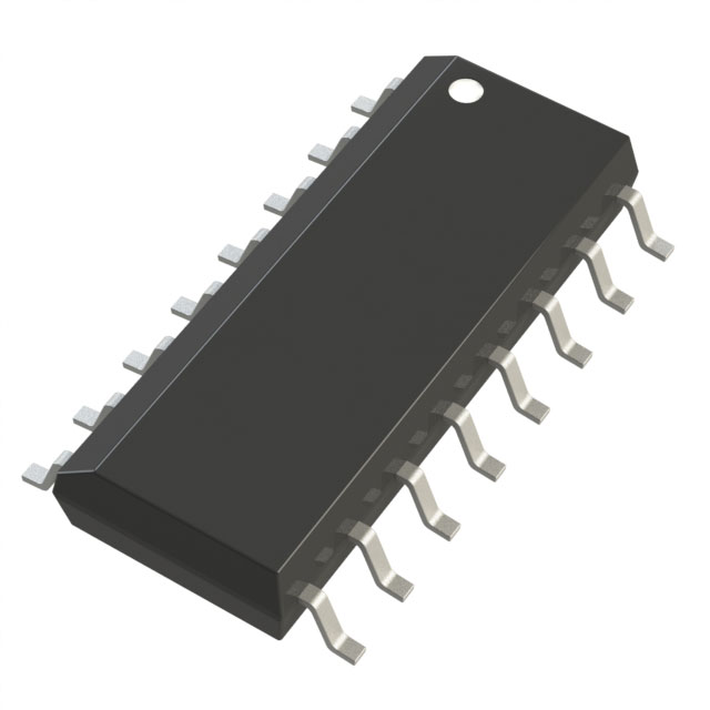
- Surface Mount Technology: The surface mount package type facilitates easy integration into compact and high-density PCB designs.
- Dual Elements: With two elements, each capable of handling 2 or 4 bits of data, the 74HCT367D,652 offers flexibility in handling multiple data lines.
- Current Handling: The device supports an output current of 6mA for both high and low states, ensuring reliable signal transmission even under load.
- Compliance and Safety: The 74HCT367D,652 is REACH unaffected and ROHS3 compliant, meeting stringent environmental and safety standards.
- Moisture Sensitivity Level: With an MSL of 1 (Unlimited), the device is suitable for use in various environmental conditions without the need for special handling.
- Packaging: The 74HCT367D,652 is available in a tube package, which is ideal for bulk handling and storage.
74HCT367D,652 Applications
The 74HCT367D,652 is ideal for applications requiring high-speed data buffering and signal conditioning. Its dual-element design makes it suitable for applications such as:
- Digital Signal Processing: Amplifying and conditioning digital signals in communication systems.
- Microcontroller Interfaces: Enhancing signal integrity when interfacing with microcontrollers and other digital devices.
- Data Transmission Lines: Buffering data lines in high-speed communication protocols.
- Computer Peripherals: Improving signal quality in interfaces such as USB, SATA, and other peripheral connections.
Conclusion of 74HCT367D,652
The 74HCT367D,652 is a versatile and reliable non-inverting buffer IC that offers high-speed performance and robust signal conditioning capabilities. Its dual-element design, surface mount package, and compliance with environmental and safety standards make it a preferred choice for a wide range of applications in the electronics industry. Despite being marked as obsolete, the 74HCT367D,652 remains a valuable component for legacy systems and applications requiring its specific features and performance benefits.
FAQ
| Quantity | Unit Price | Ext. Price |
|---|---|---|
| 10+ | $1.12115 | $11.21 |
| 50+ | $0.99943 | $49.97 |
| 100+ | $0.86228 | $86.23 |
| 500+ | $0.80057 | $400.29 |
| 1000+ | $0.77315 | $773.15 |
Not available to buy online? Want the lower wholesale price? Please Send RFQ to get best price, we will respond immediately


.png?x-oss-process=image/format,webp/resize,h_32)


