onsemi_2N7002LT1G

onsemi
2N7002LT1G  
Single FETs, MOSFETs

onsemi
2N7002LT1G
278-2N7002LT1G
Ersa
onsemi-2N7002LT1G-datasheets-1687834.pdf
MOSFET N-CH 60V 115MA SOT23-3
In Stock : 285369

Not available to buy online? Want the lower wholesale price? Please Send RFQ to get best price, we will respond immediately

QUICK RFQ
ADD TO RFQ LIST
ersa FreeSample ersa flow
  • Quantity
  • Unit Price
  • Ext. Price
    • 20+
    • $0.02936
    • $0.59
    • 200+
    • $0.02295
    • $4.59
    • 600+
    • $0.02010
    • $12.06
    • 3000+
    • $0.01797
    • $53.91
    • 9000+
    • $0.01711
    • $153.99
    • 21000+
    • $0.01654
    • $347.34
    ADD TO CART
    QUICK ORDER
    $0.00000    $0.00
    ISO9001
    Quality Policy
    ISO45001
    ISO14001

    2N7002LT1G Description

    The 2N7002LT1G is a low-voltage N-channel MOSFET transistor manufactured by ON Semiconductor. Here is a brief description of the model along with its features and applications:

    Description:

    The 2N7002LT1G is an N-channel enhancement mode field-effect transistor (MOSFET) with a low gate-to-source threshold voltage (Vth) of 2V to 4V. It is designed for low-voltage applications and offers fast switching speeds and low on-state resistance (RDS(on)).

    Features:

    1. Low gate-to-source threshold voltage (Vth) of 2V to 4V
    2. N-channel, enhancement mode
    3. Fast switching speeds
    4. Low on-state resistance (RDS(on))
    5. Suitable for low-voltage applications
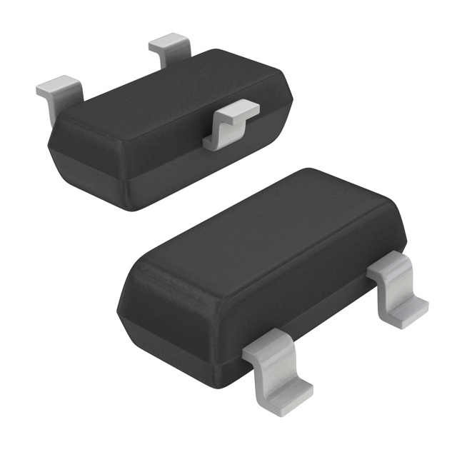
    6. Available in SOT-23 package

    Applications:

    The 2N7002LT1G is commonly used in a variety of low-voltage applications, including:

    1. Switching regulators
    2. DC-DC converters
    3. Class D audio amplifiers
    4. Battery-powered devices
    5. Low-voltage motor drivers
    6. LED drivers
    7. Power management systems

    Overall, the 2N7002LT1G is a versatile and efficient MOSFET transistor that offers excellent performance in low-voltage applications. Its low Vth, fast switching speeds, and low on-state resistance make it a popular choice for designers looking to optimize their power management systems and reduce power consumption.

    Tech Specifications

    Configuration
    Typical Turn-Off Delay Time (ns)
    Maximum Gate Source Leakage Current (nA)
    Input Capacitance (Ciss) (Max) @ Vds
    PPAP
    Channel Mode
    Typical Turn-On Delay Time (ns)
    Product Status
    Automotive
    Drain to Source Voltage (Vdss)
    Supplier Package
    Maximum IDSS (uA)
    Package / Case
    Technology
    REACH Status
    Channel Type
    EU RoHS
    Maximum Continuous Drain Current (A)
    Moisture Sensitivity Level (MSL)
    Operating Temperature
    Maximum Pulsed Drain Current @ TC=25°C (A)
    Maximum Drain Source Voltage (V)
    ECCN
    Mounting Type
    Rds On (Max) @ Id, Vgs
    Standard Package Name
    Vgs(th) (Max) @ Id
    Pin Count
    Mounting
    Minimum Gate Threshold Voltage (V)
    Typical Reverse Transfer Capacitance @ Vds (pF)
    Lead Shape
    Current - Continuous Drain (Id) @ 25°C
    Drive Voltage (Max Rds On, Min Rds On)
    HTSUS
    Package
    Maximum Drain Source Resistance (MOhm)
    Typical Input Capacitance @ Vds (pF)
    Maximum Power Dissipation on PCB @ TC=25°C (W)
    Category
    PCB changed
    HTS
    FET Type
    Number of Elements per Chip
    ECCN (US)
    Maximum Power Dissipation (mW)
    Supplier Device Package
    Minimum Operating Temperature (°C)
    Maximum Operating Temperature (°C)
    Power Dissipation (Max)
    Package Height
    Maximum Positive Gate Source Voltage (V)
    Mfr
    Vgs (Max)
    RoHS Status
    FET Feature
    Maximum Gate Source Voltage (V)
    Package Length
    Maximum Diode Forward Voltage (V)
    Series
    Operating Junction Temperature (°C)
    Typical Output Capacitance (pF)
    Part Status
    Maximum Gate Threshold Voltage (V)
    Package Width
    Maximum Junction Ambient Thermal Resistance on PCB (°C/W)
    Base Product Number
    Unit Weight
    Id - Continuous Drain Current
    Product
    RoHS
    Qg - Gate Charge
    Transistor Type
    Number of Channels
    Typical Turn-On Delay Time
    Height
    Maximum Operating Temperature
    Width
    Rds On - Drain-Source Resistance
    Mounting Style
    Vgs - Gate-Source Voltage
    Typical Turn-Off Delay Time
    Transistor Polarity
    Minimum Operating Temperature
    Vds - Drain-Source Breakdown Voltage
    Type
    Length
    Forward Transconductance - Min
    Vgs th - Gate-Source Threshold Voltage
    Pd - Power Dissipation
    USHTS

    2N7002LT1G Documents

    Download datasheets and manufacturer documentation for 2N7002LT1G

    Ersa Mult Dev Mold Comp Chg 1/Apr/2020      
    Ersa 2N7002L Datasheet      
    Ersa New taping option 15/May/2019      
    Ersa Available In the Digi-Key KiCad Library      
    Ersa 2N7002L Datasheet      
    Ersa Glue Mount Process 11/July/2008       Copper Wire 26/May/2009      
    Ersa onsemi RoHS       Material Declaration 2N7002LT1G       onsemi REACH      

    Shopping Guide

    Payment Methods
    Payment Methods include Prepayment TT (bank transfer), Western Union, and PayPal. Customers are responsible for shipping costs, bank charges, customs duties and taxes.
    Shipping Rate
    Shipments are made once a day around 5pm, excluding Sundays. Once shipped, the estimated delivery time is usually 5-7 business days, depending on the courier you choose.
    Delivery Methods
    Provide DHL, FedEx, UPS, EMS, SF Express and Registered Airmail International Delivery Service