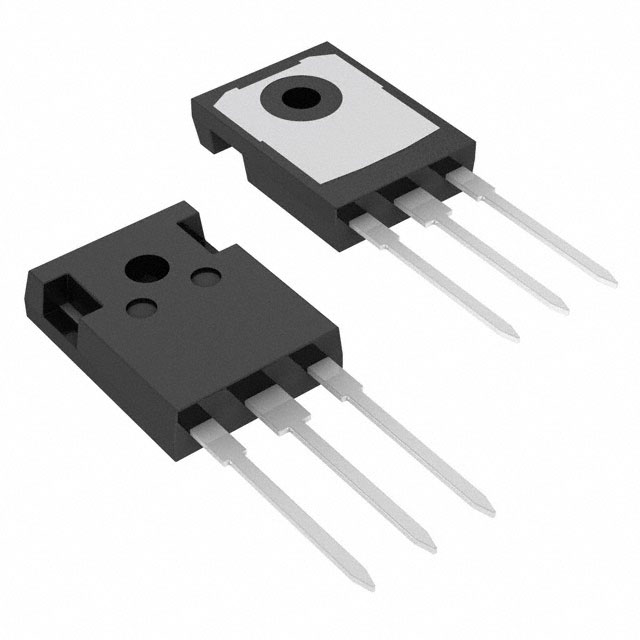
onsemi_FCH072N60F

onsemi
FCH072N60F  
Single FETs, MOSFETs

onsemi
FCH072N60F
278-FCH072N60F
Ersa
onsemi-FCH072N60F-datasheets-1832649.pdf
MOSFET N-CH 600V 52A TO247-3
In Stock : 750

Not available to buy online? Want the lower wholesale price? Please Send RFQ to get best price, we will respond immediately

QUICK RFQ
ADD TO RFQ LIST
ersa FreeSample ersa flow
ISO9001
Quality Policy
ISO45001
ISO14001

FCH072N60F Description

FCH072N60F is a high voltage N-channel MOSFET from ON Semiconductor. It is designed for use in high voltage applications and offers excellent electrical characteristics and performance.

Description:

The FCH072N60F is an N-channel enhancement mode field effect transistor. It is a three-pin device with a source, gate, and drain. The device is designed for use in high voltage applications and is suitable for use in power electronics, motor control, and other industrial applications.

Features:

  • N-channel enhancement mode MOSFET
  • High voltage rating of 600V
  • Low on-state resistance (RDS(on))
  • Fast switching speed
  • High input impedance
  • Low gate charge
  • Avalanche rugged

Applications:

The FCH072N60F is suitable for use in a wide range of applications, including:

  • Power electronics
  • Motor control
  • Industrial control
  • Switch mode power supplies (SMPS)
  • Class D audio amplifiers
  • Battery charging circuits
  • High voltage switching applications

In summary, the FCH072N60F is a high voltage N-channel MOSFET from ON Semiconductor that offers excellent electrical characteristics and performance. It is suitable for use in a wide range of high voltage applications, including power electronics, motor control, and industrial control.

Tech Specifications

FET Type
Input Capacitance (Ciss) (Max) @ Vds
Gate Charge (Qg) (Max) @ Vgs
Product Status
Supplier Device Package
Drain to Source Voltage (Vdss)
Power Dissipation (Max)
Package / Case
Technology
REACH Status
Mfr
Vgs (Max)
RoHS Status
Moisture Sensitivity Level (MSL)
Operating Temperature
FET Feature
ECCN
Mounting Type
Rds On (Max) @ Id, Vgs
Vgs(th) (Max) @ Id
Series
Current - Continuous Drain (Id) @ 25°C
Drive Voltage (Max Rds On, Min Rds On)
HTSUS
Package
Base Product Number
Typical Input Capacitance @ Vds (pF)
Category
Configuration
PCB changed
Typical Turn-Off Delay Time (ns)
HTS
Maximum Gate Source Leakage Current (nA)
Number of Elements per Chip
ECCN (US)
Typical Rise Time (ns)
PPAP
Maximum Power Dissipation (mW)
Channel Mode
Typical Turn-On Delay Time (ns)
Automotive
Minimum Operating Temperature (°C)
Maximum Operating Temperature (°C)
Supplier Package
Maximum IDSS (uA)
Typical Fall Time (ns)
Process Technology
Package Height
Channel Type
EU RoHS
Maximum Continuous Drain Current (A)
Maximum Gate Source Voltage (V)
Maximum Drain Source Voltage (V)
SVHC Exceeds Threshold
Maximum Drain Source Resistance (mOhm)
Package Length
Typical Gate Charge @ 10V (nC)
Standard Package Name
Pin Count
Mounting
Operating Junction Temperature (°C)
Tab
Lead Shape
Part Status
SVHC
Maximum Gate Threshold Voltage (V)
Package Width
Typical Gate Charge @ Vgs (nC)

FCH072N60F Documents

Download datasheets and manufacturer documentation for FCH072N60F

Shopping Guide

Payment Methods
Payment Methods include Prepayment TT (bank transfer), Western Union, and PayPal. Customers are responsible for shipping costs, bank charges, customs duties and taxes.
Shipping Rate
Shipments are made once a day around 5pm, excluding Sundays. Once shipped, the estimated delivery time is usually 5-7 business days, depending on the courier you choose.
Delivery Methods
Provide DHL, FedEx, UPS, EMS, SF Express and Registered Airmail International Delivery Service