
 German
 Japanese
 Portuguese
 Korea
Korea
 Mexico
 Dutch
Dutch


Why Choose Us?
Professional Platform
B2B & B2C purchasingDelivery at full speed
1-2 days deliveryWide variety
Original manufacturers365 days guarantee
Responsible quality
.png)


Tech Specifications
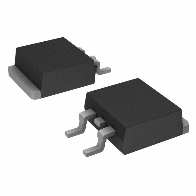
Package/Case
TO-263
Continuous Drain Current (ID)
32A
Current Rating
32A
Drain to Source Breakdown Voltage
100V
Drain to Source Resistance
32mR
Drain to Source Voltage (Vdss)
100V
Drain-source On Resistance-Max
36MR
Element Configuration
Single
FDB3682 Description
N-Channel 100 V 6A (Ta), 32A (Tc) 95W (Tc) Surface Mount TO-263 (D2PAK)
FAQ
What operating temperature range does FDB3682 support?
FDB3682 has an operating temperature range of 175°C.
What is FDB3682?
Are there related or alternative parts for FDB3682?
What voltage specification is listed for FDB3682?
What package or case is FDB3682 available in?
Quick Quote
ADD TO RFQ LIST
Not available to buy online? Want the lower wholesale price? Please Send RFQ to get best price, we will respond immediately
QUICK RFQ


.png?x-oss-process=image/format,webp/resize,h_32)


