

onsemi
FDFS2P753Z
Single FETs, MOSFETs

Not available to buy online? Want the lower wholesale price? Please Send RFQ to get best price, we will respond immediately


.png?x-oss-process=image/format,webp/resize,p_30)


FDFS2P753Z Description
FDFS2P753Z Description
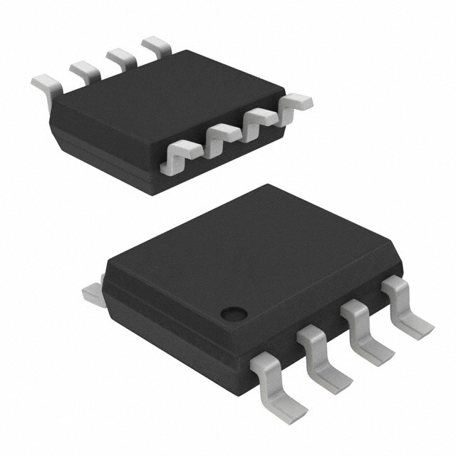
The FDFS2P753Z is a high-performance, P-channel MOSFET from onsemi, designed for applications requiring robust power management and efficient switching capabilities. With a drain-to-source voltage (Vdss) of 30V and a continuous drain current (Id) of 3A at 25°C, this device delivers exceptional performance in a compact 8SOIC package. The FDFS2P753Z is part of the PowerTrench® series, known for its advanced trench technology that provides superior switching characteristics and lower on-resistance.
FDFS2P753Z Features
- High Input Capacitance (Ciss): The FDFS2P753Z boasts a maximum input capacitance of 455 pF at 10V, ensuring fast response times and efficient signal processing.
- Low Gate Charge (Qg): With a maximum gate charge of 9.3 nC at 10V, this MOSFET minimizes power consumption during switching, contributing to energy efficiency.
- Surface Mount Technology: The FDFS2P753Z is designed for surface mount applications, allowing for compact and efficient integration into various electronic systems.
- Schottky Diode Feature: Integrated Schottky diode (isolated) provides protection against voltage spikes and reverse current, enhancing the device's reliability.
- Compliance with Regulations: The FDFS2P753Z is compliant with RoHS3 standards, making it suitable for environmentally conscious designs. It is also REACH unaffected, ensuring compliance with European chemical regulations.
FDFS2P753Z Applications
The FDFS2P753Z is ideal for applications where high voltage and current handling are required, combined with the need for efficient power management. Some specific use cases include:
- Power Management Systems: Due to its high Vdss and Id ratings, the FDFS2P753Z is well-suited for power management in various electronic devices.
- Automotive Electronics: The robustness and reliability of this MOSFET make it an excellent choice for automotive applications, such as engine control units and battery management systems.
- Industrial Control Systems: In industrial settings, the FDFS2P753Z can be used for motor control and protection circuits, where high voltage and current handling are critical.
Conclusion of FDFS2P753Z
Despite being classified as obsolete, the FDFS2P753Z remains a powerful choice for applications that can leverage its high voltage and current capabilities. Its unique features, such as the integrated Schottky diode and low gate charge, offer advantages over similar models in terms of efficiency and reliability. While it may not be the latest technology, the FDFS2P753Z continues to serve well in applications where its specific characteristics are a perfect fit.
Tech Specifications
FDFS2P753Z Documents
Download datasheets and manufacturer documentation for FDFS2P753Z
FDFS2P753Z Mult Devices 24/Oct/2017 Mult MSL1 Pkg Chg 20/Dec/2018 Mult Devices 31/Jan/2019 Logo 17/Aug/2017 Mold Compound 12/Dec/2007 onsemi RoHS onsemi REACH Related Parts


Shopping Guide


.png?x-oss-process=image/format,webp/resize,h_32)


©2025 ERSA Electronics Corporation.