

onsemi
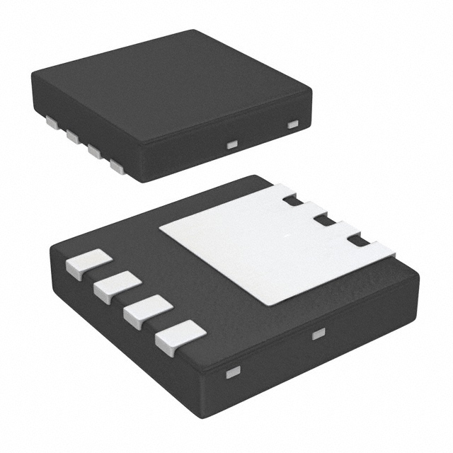
FDMC86102
Single FETs, MOSFETs

Not available to buy online? Want the lower wholesale price? Please Send RFQ to get best price, we will respond immediately


.png?x-oss-process=image/format,webp/resize,p_30)


FDMC86102 Description
FDMC86102 is a high-performance, monolithic, integrated circuit designed for use in high-speed, high-resolution, and high-accuracy optical sensing applications. It is manufactured by ON Semiconductor, a leading global supplier of semiconductor solutions.
Description:
The FDMC86102 is a fully integrated optical sensor that combines a high-speed photodiode array, a transimpedance amplifier, and a 14-bit analog-to-digital converter (ADC) in a single chip. It is designed to provide high-speed data acquisition and processing for applications that require precise measurement of light intensity.
Features:
- High-Speed Data Acquisition: The FDMC86102 can operate at sampling rates up to 1 MSPS (Million Samples Per Second), making it suitable for high-speed optical sensing applications.
- High Resolution: With a 14-bit ADC, the FDMC86102 can provide high-resolution measurements, allowing for accurate detection of small changes in light intensity.
- Integrated Photodiode Array: The device features an integrated photodiode array, eliminating the need for external photodiodes and simplifying the overall system design.
- Transimpedance Amplifier: The built-in transimpedance amplifier provides a high gain and low noise amplification of the photodiode signal, improving the overall sensitivity and accuracy of the sensor.
- Programmable Gain: The gain of the transimpedance amplifier can be programmed, allowing for flexibility in adjusting the sensitivity of the sensor to different light levels.
- Small Package: The FDMC86102 is available in a compact 48-pin QFN package, making it suitable for space-constrained applications.
Applications:
- Spectroscopy: The FDMC86102 can be used in spectroscopic applications for precise measurement of light intensity across a wide range of wavelengths.
- Optical Sensing: The device is well-suited for high-speed, high-accuracy optical sensing applications, such as laser-based distance measurement or optical communication systems.
- Machine Vision: The FDMC86102 can be used in machine vision systems for accurate detection and measurement of light patterns, enabling applications like object recognition, quality control, and robotics.
- Biomedical Imaging: The high-speed and high-resolution capabilities of the FDMC86102 make it suitable for use in biomedical imaging systems, such as fluorescence microscopy or optical coherence tomography.
- Environmental Monitoring: The device can be used in environmental monitoring systems for detecting and measuring light pollution, solar radiation, or other light-related parameters.
In summary, the FDMC86102 is a high-performance optical sensor IC that offers high-speed data acquisition, high resolution, and integrated photodiode array in a compact package. It is suitable for a wide range of applications, including spectroscopy, optical sensing, machine vision, biomedical imaging, and environmental monitoring.
Tech Specifications
FDMC86102 Documents
Download datasheets and manufacturer documentation for FDMC86102
Wafer 6/8 Inch Addition 16/Jun/2014 FDMC86102 Mult Devices 24/Oct/2017 Logo 17/Aug/2017 onsemi RoHS Material Declaration FDMC86102 Related Parts


Shopping Guide


.png?x-oss-process=image/format,webp/resize,h_32)


©2025 ERSA Electronics Corporation.