
 German
 Japanese
 Portuguese
 Korea
Korea
 Mexico
 Dutch
Dutch


onsemi
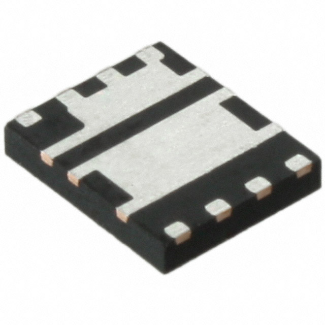
FDMS3669S
289-FDMS3669S

PDF Datasheet
Asymmetric Dual N-Channel PowerTrench® Power Stage MOSFET 30V, 3000-REEL
52 Weeks
Why Choose Us?
Professional Platform
B2B & B2C purchasingDelivery at full speed
1-2 days deliveryWide variety
Original manufacturers365 days guarantee
Responsible quality
.png)


Tech Specifications
Continuous Drain Current (ID)
60A
Drain to Source Resistance
10mR
Drain to Source Voltage (Vdss)
30V
Fall Time
3ns
FET Type
2 N-Channel
Gate to Source Voltage (Vgs)
20V
Height
1.1mm
Input Capacitance
1.605nF
FDMS3669S Description
FDMS3669S is a high-power discrete transistor offered by ON Semiconductor. It is a NPN Darlington transistor that is designed for high-power applications.
Description:
The FDMS3669S is a high-power NPN Darlington transistor that features high current gain, high voltage gain, and high power dissipation capabilities. It is available in a TO-247AC package, which is suitable for high-power applications.
Features:
- High current gain (hFE) of 5000 minimum
- High voltage gain (hFE) of 30,000 minimum
- High power dissipation capability of 150 watts
- Collector-emitter voltage (VCEO) of 1500 volts
- Collector-base voltage (VCBO) of 1500 volts
- Emitter-base voltage (VEBO) of 6 volts
- Low saturation voltage (VCE(sat)) of 2 volts maximum
- High switching speed
- High thermal resistance
Applications:
The FDMS3669S is suitable for a wide range of high-power applications, including:
- Power switching and amplification in industrial control systems
- Motor control and drive systems
- Power supplies and inverters
- Audio amplifiers and loudspeaker drivers
- Automotive and motorcycle ignition systems
- High-power switching and amplification in renewable energy systems
It is important to note that the FDMS3669S is a high-power transistor and should be used with appropriate heat sinking and driving circuitry to ensure safe and reliable operation. Additionally, proper design and layout considerations should be taken into account to minimize parasitic inductance and ensure optimal performance.
FAQ
What operating temperature range does FDMS3669S support?
FDMS3669S has an operating temperature range of 150°C.
What is the mounting type of FDMS3669S?
Are there related or alternative parts for FDMS3669S?
What is the standard lead time for FDMS3669S?
Is FDMS3669S currently in stock?
Quick Quote
ADD TO RFQ LIST
Not available to buy online? Want the lower wholesale price? Please Send RFQ to get best price, we will respond immediately
QUICK RFQ


.png?x-oss-process=image/format,webp/resize,h_32)


