
 German
 Japanese
 Portuguese
 Korea
Korea
 Mexico
 Dutch
Dutch


onsemi
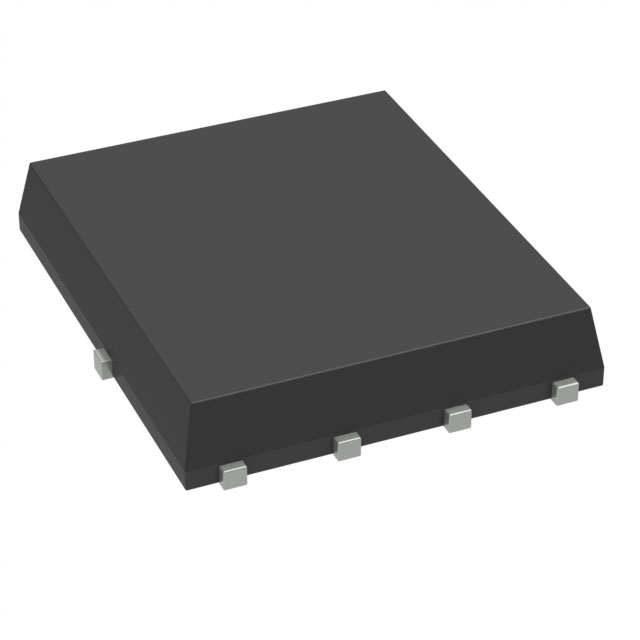
FDMS7650

Why Choose Us?
Professional Platform
B2B & B2C purchasingDelivery at full speed
1-2 days deliveryWide variety
Original manufacturers365 days guarantee
Responsible quality
.png)


Tech Specifications
FDMS7650 Description
The FDMS7650 is a high-performance, dual N-channel MOSFET driver from ON Semiconductor. It is designed to drive power MOSFETs in a wide range of applications, including motor control, power management, and automotive systems.
Description:
The FDMS7650 is a monolithic integrated circuit that provides two high-speed N-channel MOSFET drivers in a single package. It features high output current capability, low propagation delay, and excellent noise immunity. The device also includes integrated protection features such as overcurrent protection, undervoltage lockout, and open-drain, open-collector output stage.
Features:
- Dual high-speed N-channel MOSFET drivers
- High output current capability (up to ±1.5A)
- Low propagation delay (down to 45ns)
- Excellent noise immunity (up to 25V/µs)
- Integrated overcurrent protection
- Undervoltage lockout
- Open-drain, open-collector output stage
- Wide operating voltage range (4.5V to 18V)
- Small package size (SOIC-8 or TSSOP-8)
Applications:
- Motor control systems
- Power management systems
- Automotive systems
- Switch mode power supplies (SMPS)
- Class D audio amplifiers
- DC-DC converters
- Battery management systems (BMS)
- Industrial control systems
- Renewable energy systems
In summary, the FDMS7650 is a versatile and high-performance MOSFET driver that is well-suited for a wide range of applications requiring high-speed switching and robust protection features. Its small package size and wide operating voltage range make it an ideal choice for space-constrained and power-sensitive applications.
FAQ
Not available to buy online? Want the lower wholesale price? Please Send RFQ to get best price, we will respond immediately


.png?x-oss-process=image/format,webp/resize,h_32)


