
 German
 Japanese
 Portuguese
 Korea
Korea
 Mexico
 Dutch
Dutch


onsemi
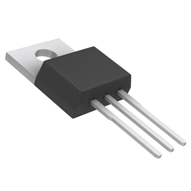
FDP070AN06A0
278-FDP070AN06A0

PDF Datasheet
N-Ch MOSFET 60V 80A 7mR TO-220 PowerTrench
15 Weeks
Why Choose Us?
Professional Platform
B2B & B2C purchasingDelivery at full speed
1-2 days deliveryWide variety
Original manufacturers365 days guarantee
Responsible quality
.png)


Tech Specifications
Package/Case
TO-220-3
Continuous Drain Current (ID)
80A
Current Rating
80A
Drain to Source Breakdown Voltage
60V
Drain to Source Resistance
7mR
Drain to Source Voltage (Vdss)
60V
Element Configuration
Single
Fall Time
35ns
FDP070AN06A0 Description
N-Channel 60 V 15A (Ta), 80A (Tc) 175W (Tc) Through Hole TO-220-3
FAQ
Is FDP070AN06A0 currently in stock?
Yes. FDP070AN06A0 currently shows 561 unit(s) in stock.
Are there related or alternative parts for FDP070AN06A0?
What is FDP070AN06A0?
What voltage specification is listed for FDP070AN06A0?
What operating temperature range does FDP070AN06A0 support?
Quick Quote
ADD TO RFQ LIST
Not available to buy online? Want the lower wholesale price? Please Send RFQ to get best price, we will respond immediately
QUICK RFQ


.png?x-oss-process=image/format,webp/resize,h_32)


