
onsemi
FDS8949-F085
FET, MOSFET Arrays


.png?x-oss-process=image/format,webp/resize,p_30)


FDS8949-F085 Description
The FDS8949-F085 is a high-performance, integrated MOSFET driver from ON Semiconductor. It is designed to drive N-channel and P-channel MOSFETs in a variety of applications, including motor control, power management, and automotive systems.
Description:
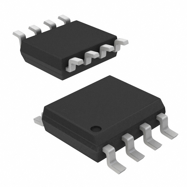
The FDS8949-F085 is a monolithic high-voltage MOSFET driver that features a high-voltage input protection and a low-voltage output stage. It is available in a compact SOIC-8 package, making it suitable for space-constrained applications.
Features:
- High-voltage input protection
- Low-voltage output stage
- Wide operating voltage range (4.5V to 40V)
- Short-circuit protection
- Over-temperature protection
- Enable control with active low input
- Open-drain output for communication with microcontrollers
- Internal charge pump for bootstrap applications
Applications:
- Motor control
- Power management
- Automotive systems
- Industrial control
- Battery management systems
- Class D audio amplifiers
- DC-DC converters
The FDS8949-F085 is a versatile MOSFET driver that offers high performance and reliability in a range of applications. Its features, such as high-voltage input protection and over-temperature protection, make it an ideal choice for applications that require high levels of safety and reliability. Additionally, its wide operating voltage range and enable control make it suitable for a variety of power management and motor control applications.
Tech Specifications
FDS8949-F085 Documents
Download datasheets and manufacturer documentation for FDS8949-F085
 Mult Device Part Number Chg 30/May/2017
  FDS8949_F085
  Mult Devices 24/Oct/2017 MSL1 Pkg Chg 20/Dec/2018
  On Semiconductor Automotive F085 Status Check
  Mult Dev EOL 20/Dec/2021 4Q2019 EOL 1/Apr/2020
  FDS8949_F085
  Logo 17/Aug/2017
  onsemi RoHS onsemi REACH Material Declaration FDS8949-F085
 Shopping Guide


.png?x-oss-process=image/format,webp/resize,h_32)


