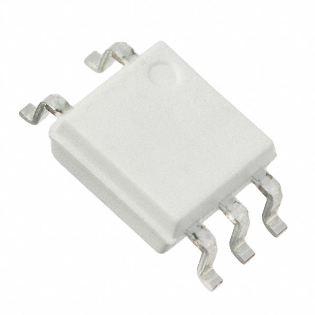
onsemi_FODM8061V

onsemi
FODM8061V  
Logic Output Optoisolators

onsemi
FODM8061V
902-FODM8061V
Ersa
onsemi-FODM8061V-datasheets-9353479.pdf
OPTOISO 3.75KV OPEN COLL 5MFP
In Stock : 3000

Not available to buy online? Want the lower wholesale price? Please Send RFQ to get best price, we will respond immediately

QUICK RFQ
ADD TO RFQ LIST
ersa FreeSample ersa flow
ISO9001
Quality Policy
ISO45001
ISO14001

FODM8061V Description

This FODM8061V belongs to Logic Output Optoisolators category. And its highest category level is Isolators. Logic Output Optoisolators category is subject to isolators. A mechanical switch known as an isolator isolates the substation's problematic area. In order to prevent the occurrence of serious flaws, this "FODM8061V" is used to divide a damaged area. A damaged area needs to be repaired from a healthy section. onsemi generates this FODM8061V. And it decides to upgrade this chip to meet consumers’ demand. onsemi is committed to be at the forefront of electronic component technology. The Tube is tailored to shape and size of the FODM8061V. The design of the FODM8061V packaging can keep the product from going bad and decrease costs. This electronic component’s applications involve high voltage devices such as transformers.

Tech Specifications

Inputs - Side 1/Side 2
Rise / Fall Time (Typ)
Output Type
Common Mode Transient Immunity (Min)
Product Status
Supplier Device Package
Data Rate
Package / Case
Number of Channels
Voltage - Supply
REACH Status
Mfr
Voltage - Forward (Vf) (Typ)
Propagation Delay tpLH / tpHL (Max)
RoHS Status
Moisture Sensitivity Level (MSL)
Operating Temperature
Input Type
Voltage - Isolation
ECCN
Mounting Type
Series
HTSUS
Package
Current - Output / Channel
Current - DC Forward (If) (Max)
Base Product Number
Number of Channels per Chip
PCB changed
Minimum Isolation Voltage (Vrms)
HTS
ECCN (US)
PPAP
Standard
Maximum Power Dissipation (mW)
Automotive
Direction Type
Typical Rise Time (us)
Maximum Data Rate
Minimum Operating Temperature (°C)
Maximum Operating Temperature (°C)
Supplier Package
Package Height
Typical Forward Voltage (V)
Polarity
Maximum Reverse Voltage (V)
EU RoHS
Maximum Forward Current (mA)
Maximum Forward Voltage (V)
Minimum Forward Voltage (V)
Maximum Propagation Delay Time (ns)
Typical Fall Time (us)
Package Length
Standard Package Name
Pin Count
Mounting
Part Status
Maximum Continuous Output Current (mA)
Package Width

FODM8061V Documents

Download datasheets and manufacturer documentation for FODM8061V

Ersa Mult DEV Mold/Die/Mat 18/Dec/2023      
Ersa FODM8061      
Ersa Mult Devices 24/Oct/2017      
Ersa FODM8061      
Ersa Logo 17/Aug/2017       Material Change 03/Mar/2023      
Ersa Material Declaration FODM8061V      

Shopping Guide

Payment Methods
Payment Methods include Prepayment TT (bank transfer), Western Union, and PayPal. Customers are responsible for shipping costs, bank charges, customs duties and taxes.
Shipping Rate
Shipments are made once a day around 5pm, excluding Sundays. Once shipped, the estimated delivery time is usually 5-7 business days, depending on the courier you choose.
Delivery Methods
Provide DHL, FedEx, UPS, EMS, SF Express and Registered Airmail International Delivery Service