
 German
 Japanese
 Portuguese
 Korea
Korea
 Mexico
 Dutch
Dutch


onsemi
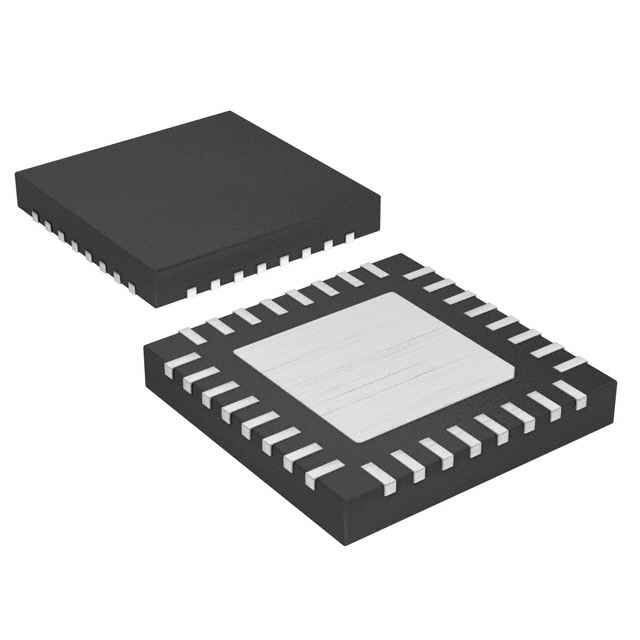
MC100LVEP210MNG

Why Choose Us?
Professional Platform
B2B & B2C purchasingDelivery at full speed
1-2 days deliveryWide variety
Original manufacturers365 days guarantee
Responsible quality
.png)


Tech Specifications
MC100LVEP210MNG Description
MC100LVEP210MNG Description
The MC100LVEP210MNG is a high-performance clock buffer designed for precision signal distribution in demanding electronic systems. Manufactured by onsemi, this device is part of the 100LVEP series and features a 1:5 input-to-output ratio, making it ideal for applications requiring fanout buffering. The device supports a wide range of input and output signal types, including ECL, HSTL, LVDS, and PECL, ensuring compatibility with various system architectures. With a maximum operating frequency of 3 GHz, the MC100LVEP210MNG is well-suited for high-speed clock distribution tasks.
MC100LVEP210MNG Features
- Input and Output Compatibility: The MC100LVEP210MNG supports multiple input and output signal types, including ECL, HSTL, LVDS, and PECL, providing flexibility in system design.
- High-Speed Performance: With a maximum frequency of 3 GHz, this clock buffer ensures minimal signal degradation and high reliability in high-speed applications.
- Differential Signaling: The device supports differential signaling for both input and output, which enhances signal integrity and reduces electromagnetic interference (EMI).
- Supply Voltage Range: The MC100LVEP210MNG operates within a supply voltage range of 2.375V to 3.8V, offering compatibility with various power supply configurations.
- Surface Mount Technology: The surface mount mounting type simplifies assembly processes and enhances board density.
- Moisture Sensitivity Level: With an MSL rating of 1 (Unlimited), the device is suitable for a wide range of manufacturing environments without the need for special handling.
- Compliance and Safety: The MC100LVEP210MNG is REACH unaffected and classified under HTSUS code 8542.39.0001, ensuring compliance with international regulations.
MC100LVEP210MNG Applications
The MC100LVEP210MNG is ideal for a variety of applications where high-speed clock distribution and signal integrity are critical. Key applications include:
- Telecommunications: High-speed clock distribution in base stations and network equipment.
- Data Centers: Ensuring reliable clock signals in server and storage systems.
- Industrial Automation: Precision timing in control systems and robotic applications.
- Medical Equipment: Reliable clock distribution in diagnostic and monitoring devices.
- High-Performance Computing: Efficient clock buffering in supercomputers and data processing units.
Conclusion of MC100LVEP210MNG
The MC100LVEP210MNG is a versatile and high-performance clock buffer that offers significant advantages in high-speed signal distribution. Its wide range of input and output compatibility, differential signaling, and high operating frequency make it a robust solution for various electronic systems. Despite being marked as obsolete, the MC100LVEP210MNG remains a reliable choice for applications requiring precision and reliability. Its compliance with international standards and safety regulations further enhances its suitability for diverse industrial and commercial applications.
FAQ
Not available to buy online? Want the lower wholesale price? Please Send RFQ to get best price, we will respond immediately


.png?x-oss-process=image/format,webp/resize,h_32)


