
 German
 Japanese
 Portuguese
 Korea
Korea
 Mexico
 Dutch
Dutch


onsemi
MJD45H11-1G

Why Choose Us?
Professional Platform
B2B & B2C purchasingDelivery at full speed
1-2 days deliveryWide variety
Original manufacturers365 days guarantee
Responsible quality
.png)


Tech Specifications
MJD45H11-1G Description
MJD45H11-1G Description
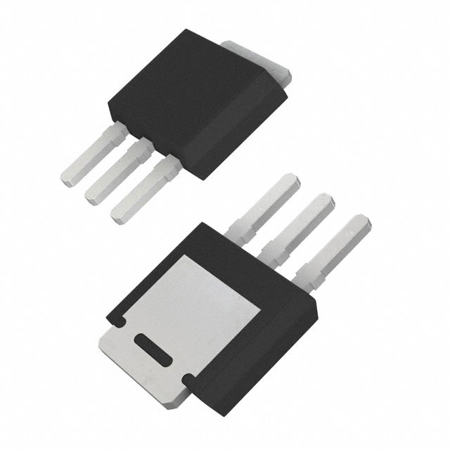
The MJD45H11-1G is a high-performance PNP bipolar transistor designed and manufactured by onsemi. It is a single Bipolar Transistor with a 90MHz frequency transition, making it suitable for high-frequency applications. The device offers a maximum collector current (Ic) of 8 A and a maximum collector-emitter breakdown voltage of 80 V. The MJD45H11-1G is designed for through-hole mounting and comes in a tube package.
MJD45H11-1G Features
- High Frequency Transition: With a 90MHz frequency transition, the MJD45H11-1G is ideal for high-frequency applications.
- High Collector Current: The device can handle a maximum collector current of 8 A, making it suitable for power applications.
- Low Vce Saturation: The MJD45H11-1G has a low Vce saturation voltage of 1V at 400mA and 8A, ensuring efficient operation.
- High DC Current Gain: The device offers a minimum DC current gain (hFE) of 40 at 4A and 1V, providing excellent performance.
- RoHS Compliance: The MJD45H11-1G is compliant with RoHS3 standards, making it suitable for environmentally friendly applications.
- REACH Unaffected: The device is not affected by REACH regulations, ensuring compliance with European chemical legislation.
MJD45H11-1G Applications
The MJD45H11-1G is ideal for a wide range of applications, including:
- Power Amplifiers: Due to its high collector current and low Vce saturation, the MJD45H11-1G is suitable for power amplifiers in audio and communication systems.
- Switching Applications: The device's high-frequency transition and low Vce saturation make it ideal for switching applications in power supplies and motor control systems.
- RF Amplifiers: The 90MHz frequency transition allows the MJD45H11-1G to be used in RF amplifiers for wireless communication systems.
Conclusion of MJD45H11-1G
The MJD45H11-1G is a versatile and high-performance PNP bipolar transistor designed for high-frequency and power applications. Its unique features, such as high collector current, low Vce saturation, and high DC current gain, make it an ideal choice for power amplifiers, switching applications, and RF amplifiers. With its RoHS compliance and REACH unaffected status, the MJD45H11-1G is also suitable for environmentally friendly applications. Overall, the MJD45H11-1G offers excellent performance and reliability in a wide range of applications.
FAQ
| Quantity | Unit Price | Ext. Price |
|---|---|---|
| 10+ | $0.56572 | $5.66 |
| 30+ | $0.50400 | $15.12 |
| 75+ | $0.43715 | $32.79 |
| 525+ | $0.39943 | $209.70 |
| 975+ | $0.37885 | $369.38 |
Not available to buy online? Want the lower wholesale price? Please Send RFQ to get best price, we will respond immediately


.png?x-oss-process=image/format,webp/resize,h_32)


