
 German
 Japanese
 Portuguese
 Korea
Korea
 Mexico
 Dutch
Dutch


onsemi
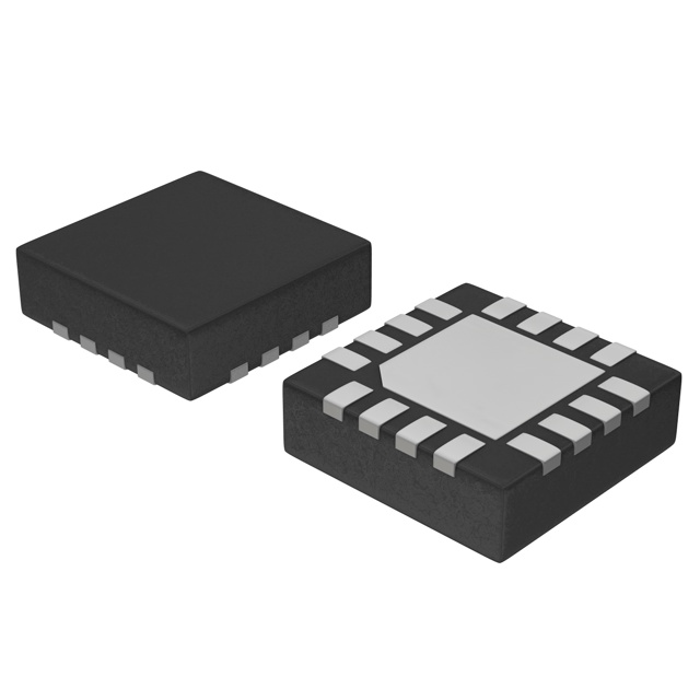
NB3L202KMNG

Why Choose Us?
Professional Platform
B2B & B2C purchasingDelivery at full speed
1-2 days deliveryWide variety
Original manufacturers365 days guarantee
Responsible quality
.png)


Tech Specifications
NB3L202KMNG Description
NB3L202KMNG Description
The NB3L202KMNG from onsemi is a high-performance 1:2 fanout buffer designed for precision clock distribution in demanding electronic systems. This surface-mount IC supports a wide input voltage range of 2.375V to 3.63V and delivers HCSL outputs with exceptional signal integrity. It accepts multiple input types, including HCSL, LVCMOS, LVDS, LVPECL, and LVTTL, making it highly versatile for diverse clocking applications. With a maximum frequency of 350 MHz, it ensures low-jitter signal propagation, critical for high-speed data communication and synchronization. Packaged in a 16-QFN tube, it is RoHS3 compliant and rated MSL 1 (Unlimited), ensuring reliability in manufacturing and operation.
NB3L202KMNG Features
- Flexible Input Compatibility: Supports HCSL, LVCMOS, LVDS, LVPECL, and LVTTL inputs, enabling seamless integration with various clock sources.
- Low-Jitter Performance: Optimized for 350 MHz operation with minimal phase noise, ideal for high-speed systems.
- Differential I/O: Features differential input and output (Yes/Yes), enhancing noise immunity and signal fidelity.
- Wide Supply Range: Operates from 2.375V to 3.63V, accommodating mixed-voltage environments.
- Compact & Reliable: 16-QFN package with REACH unaffected and RoHS3 compliance, suitable for space-constrained designs.
- Industrial Robustness: EAR99 classification and unlimited MSL rating ensure durability in harsh conditions.
NB3L202KMNG Applications
- Telecommunications: Clock distribution in 5G base stations, routers, and switches requiring low-jitter signals.
- Data Centers: Synchronization of high-speed SerDes, FPGAs, and ASICs in server and storage systems.
- Test & Measurement: Precision timing for oscilloscopes, signal generators, and ATE equipment.
- Consumer Electronics: Clock management in gaming consoles, high-end displays, and audio/video interfaces.
- Automotive & Industrial: Reliable timing for ADAS, infotainment, and industrial automation where signal integrity is critical.
Conclusion of NB3L202KMNG
The NB3L202KMNG stands out as a robust, high-performance clock buffer, combining multi-standard input support, low jitter, and differential signaling in a compact form factor. Its wide voltage range and industrial-grade reliability make it a preferred choice for applications demanding precise clock distribution. Whether in telecom infrastructure, data centers, or automotive systems, this IC delivers unmatched performance, ensuring synchronization accuracy and system stability.
FAQ
| Quantity | Unit Price | Ext. Price |
|---|---|---|
| 1+ | $8.00228 | $8.00 |
| 10+ | $6.80915 | $68.09 |
| 30+ | $6.08228 | $182.47 |
Not available to buy online? Want the lower wholesale price? Please Send RFQ to get best price, we will respond immediately


.png?x-oss-process=image/format,webp/resize,h_32)


